Home > Press > Researchers gauge quantum properties of nanotubes, essential for next-gen electronics: Imaging method allowed researchers to measure the nanotube quantum capacitance-a very unique property of an object from the nano-world
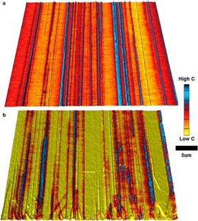 |
| (a, b) MIM capacitance images overlaid on top of AFM 3-D surface topography of an array of CVD grown aligned SWNTs on quartz substrates. Each sample has a 3.5 nm dielectric layer of (a) MgO and (b) SiO2. The impact of the increased ε for MgO is apparent, resulting in improved contrast and uniformity. CREDIT: John A. Rogers, Eric Seabron, Scott MacLaren and Xu Xie from the University of Illinois at Urbana-Champaign; Slava V. Rotkin from Lehigh University; and, William L. Wilson from Harvard University |
Abstract:
How do you get to know a material that you cannot see?
That is a question that researchers studying nanomaterials--objects with features at the sub-micrometer scales such as quantum dots, nanoparticles and nanotubes--are seeking to answer.
Researchers gauge quantum properties of nanotubes, essential for next-gen electronics: Imaging method allowed researchers to measure the nanotube quantum capacitance-a very unique property of an object from the nano-world
Bethlehem, PA | Posted on January 8th, 2016Though recent discoveries--including a super-resolution microscopy which won the Nobel Prize in 2014--have greatly enhanced scientists' capacity to use light to learn about these small-scale objects, the wavelength of the inspecting radiation is always much larger than the scale of the nano-objects being studied. For example, nanotubes and nanowires-the building blocks of next-generation electronic devices-have diameters that are hundreds of times smaller than the light could resolve. Researchers must find ways to circumvent this physical limitation in order to achieve sub-wavelength spatial resolution and explore the nature of these materials for future computers.
Today, a group of scientists--John A. Rogers, Eric Seabron, Scott MacLaren and Xu Xie from the University of Illinois at Urbana-Champaign; Slava V. Rotkin from Lehigh University; and, William L. Wilson from Harvard University--are reporting on the discovery of an important method for measuring the properties of nanotube materials using a microwave probe. Their findings have been published in ACS Nano in an article called: "Scanning Probe Microwave Reflectivity of Aligned Single-Walled Carbon Nanotubes: Imaging of Electronic Structure and Quantum Behavior at the Nanoscale."
The researchers studied single-walled carbon nanotubes. These are 1-dimensional, wire-like nanomaterials that have electronic properties that make them excellent candidates for next generation electronics technologies. In fact, the first prototype of a nanotube computer has already been built by researchers at Stanford University. The IBM T.J. Watson Research Center is currently developing nanotube transistors for commercial use.
For this study, scientists grew a series of parallel nanotube lines, similar to the way nanotubes will be used in computer chips. Each nanotube was about 1 nanometer wide--ten times smaller than expected for use in the next generation of electronics. To explore the material's properties, they then used microwave impedance microscopy (MIM) to image individual nanotubes.
"Although microwave near-field imaging offers an extremely versatile 'nondestructive' tool for characterizing materials, it is not an immediately obvious choice," explained Rotkin, a professor with a dual appointment in Lehigh's Department of Physics and Department of Materials Science and Engineering. "Indeed, the wavelength of the radiation used in the experiment was even longer than what is typically used in optical microscopy-about 12 inches, which is approximately 100,000,000 times larger than the nanotubes we measured."
He added: "The nanotube, in this case, is like a very bright needle in a very large haystack."
The imaging method they developed shows exactly where the nanotubes are on the silicon chip. More importantly, the information delivered by the microwave signal from individual nanotubes revealed which nanotubes were and were not able to conduct electric current. Unexpectedly, they were finally able to measure the nanotube quantum capacitance-a very unique property of an object from the nano-world-under these experimental conditions.
"We began our collaboration seeking to understand the images taken by the microwave microscopy and ended by unveiling the nanotube's quantum behavior, which can now be measured with atomistic resolution," said Rotkin.
As an inspection tool or metrology technique, this approach could have a tremendous impact on future technologies, allowing optimization of processing strategies including scalable enriched nanotube growth, post-growth purification, and fabrication of better device contacts. One can now distinguish, in one simple step, between semiconductor nanotubes that are useful for electronics and metallic ones that can cause a computer to failure. Moreover this set of imaging modes sheds light on the quantum properties of these 1D structures.
####
For more information, please click here
Contacts:
Lori Friedman
323-377-4312
Copyright © Lehigh University
If you have a comment, please Contact us.Issuers of news releases, not 7th Wave, Inc. or Nanotechnology Now, are solely responsible for the accuracy of the content.
Bookmark:


| Related Links |
| Related News Press |
News and information
![]() Quantum computer improves AI predictions April 17th, 2026
Quantum computer improves AI predictions April 17th, 2026
![]() Flexible sensor gains sensitivity under pressure April 17th, 2026
Flexible sensor gains sensitivity under pressure April 17th, 2026
![]() A reusable chip for particulate matter sensing April 17th, 2026
A reusable chip for particulate matter sensing April 17th, 2026
![]() Detecting vibrational quantum beating in the predissociation dynamics of SF6 using time-resolved photoelectron spectroscopy April 17th, 2026
Detecting vibrational quantum beating in the predissociation dynamics of SF6 using time-resolved photoelectron spectroscopy April 17th, 2026
Imaging
![]() Simple algorithm paired with standard imaging tool could predict failure in lithium metal batteries August 8th, 2025
Simple algorithm paired with standard imaging tool could predict failure in lithium metal batteries August 8th, 2025
Possible Futures
![]() A fundamentally new therapeutic approach to cystic fibrosis: Nanobody repairs cellular defect April 17th, 2026
A fundamentally new therapeutic approach to cystic fibrosis: Nanobody repairs cellular defect April 17th, 2026
![]() UC Irvine physicists discover method to reverse �quantum scrambling� : The work addresses the problem of information loss in quantum computing system April 17th, 2026
UC Irvine physicists discover method to reverse �quantum scrambling� : The work addresses the problem of information loss in quantum computing system April 17th, 2026
Nanotubes/Buckyballs/Fullerenes/Nanorods/Nanostrings/Nanosheets
![]() Tiny nanosheets, big leap: A new sensor detects ethanol at ultra-low levels January 30th, 2026
Tiny nanosheets, big leap: A new sensor detects ethanol at ultra-low levels January 30th, 2026
![]() Enhancing power factor of p- and n-type single-walled carbon nanotubes April 25th, 2025
Enhancing power factor of p- and n-type single-walled carbon nanotubes April 25th, 2025
![]() Chainmail-like material could be the future of armor: First 2D mechanically interlocked polymer exhibits exceptional flexibility and strength January 17th, 2025
Chainmail-like material could be the future of armor: First 2D mechanically interlocked polymer exhibits exceptional flexibility and strength January 17th, 2025
![]() Innovative biomimetic superhydrophobic coating combines repair and buffering properties for superior anti-erosion December 13th, 2024
Innovative biomimetic superhydrophobic coating combines repair and buffering properties for superior anti-erosion December 13th, 2024
Nanoelectronics
![]() Lab to industry: InSe wafer-scale breakthrough for future electronics August 8th, 2025
Lab to industry: InSe wafer-scale breakthrough for future electronics August 8th, 2025
![]() Interdisciplinary: Rice team tackles the future of semiconductors Multiferroics could be the key to ultralow-energy computing October 6th, 2023
Interdisciplinary: Rice team tackles the future of semiconductors Multiferroics could be the key to ultralow-energy computing October 6th, 2023
![]() Key element for a scalable quantum computer: Physicists from Forschungszentrum J�lich and RWTH Aachen University demonstrate electron transport on a quantum chip September 23rd, 2022
Key element for a scalable quantum computer: Physicists from Forschungszentrum J�lich and RWTH Aachen University demonstrate electron transport on a quantum chip September 23rd, 2022
![]() Reduced power consumption in semiconductor devices September 23rd, 2022
Reduced power consumption in semiconductor devices September 23rd, 2022
Discoveries
![]() Quantum computer improves AI predictions April 17th, 2026
Quantum computer improves AI predictions April 17th, 2026
![]() Flexible sensor gains sensitivity under pressure April 17th, 2026
Flexible sensor gains sensitivity under pressure April 17th, 2026
![]() A reusable chip for particulate matter sensing April 17th, 2026
A reusable chip for particulate matter sensing April 17th, 2026
![]() Detecting vibrational quantum beating in the predissociation dynamics of SF6 using time-resolved photoelectron spectroscopy April 17th, 2026
Detecting vibrational quantum beating in the predissociation dynamics of SF6 using time-resolved photoelectron spectroscopy April 17th, 2026
Materials/Metamaterials/Magnetoresistance
![]() First real-time observation of two-dimensional melting process: Researchers at Mainz University unveil new insights into magnetic vortex structures August 8th, 2025
First real-time observation of two-dimensional melting process: Researchers at Mainz University unveil new insights into magnetic vortex structures August 8th, 2025
![]() Researchers unveil a groundbreaking clay-based solution to capture carbon dioxide and combat climate change June 6th, 2025
Researchers unveil a groundbreaking clay-based solution to capture carbon dioxide and combat climate change June 6th, 2025
![]() A 1960s idea inspires NBI researchers to study hitherto inaccessible quantum states June 6th, 2025
A 1960s idea inspires NBI researchers to study hitherto inaccessible quantum states June 6th, 2025
![]() Institute for Nanoscience hosts annual proposal planning meeting May 16th, 2025
Institute for Nanoscience hosts annual proposal planning meeting May 16th, 2025
Announcements
![]() A fundamentally new therapeutic approach to cystic fibrosis: Nanobody repairs cellular defect April 17th, 2026
A fundamentally new therapeutic approach to cystic fibrosis: Nanobody repairs cellular defect April 17th, 2026
![]() UC Irvine physicists discover method to reverse �quantum scrambling� : The work addresses the problem of information loss in quantum computing system April 17th, 2026
UC Irvine physicists discover method to reverse �quantum scrambling� : The work addresses the problem of information loss in quantum computing system April 17th, 2026
Interviews/Book Reviews/Essays/Reports/Podcasts/Journals/White papers/Posters
![]() A fundamentally new therapeutic approach to cystic fibrosis: Nanobody repairs cellular defect April 17th, 2026
A fundamentally new therapeutic approach to cystic fibrosis: Nanobody repairs cellular defect April 17th, 2026
![]() UC Irvine physicists discover method to reverse �quantum scrambling� : The work addresses the problem of information loss in quantum computing system April 17th, 2026
UC Irvine physicists discover method to reverse �quantum scrambling� : The work addresses the problem of information loss in quantum computing system April 17th, 2026
Tools
![]() Metasurfaces smooth light to boost magnetic sensing precision January 30th, 2026
Metasurfaces smooth light to boost magnetic sensing precision January 30th, 2026
![]() From sensors to smart systems: the rise of AI-driven photonic noses January 30th, 2026
From sensors to smart systems: the rise of AI-driven photonic noses January 30th, 2026
![]() Japan launches fully domestically produced quantum computer: Expo visitors to experience quantum computing firsthand August 8th, 2025
Japan launches fully domestically produced quantum computer: Expo visitors to experience quantum computing firsthand August 8th, 2025
Quantum Dots/Rods
![]() A new kind of magnetism November 17th, 2023
A new kind of magnetism November 17th, 2023
![]() IOP Publishing celebrates World Quantum Day with the announcement of a special quantum collection and the winners of two prestigious quantum awards April 14th, 2023
IOP Publishing celebrates World Quantum Day with the announcement of a special quantum collection and the winners of two prestigious quantum awards April 14th, 2023
![]() Qubits on strong stimulants: Researchers find ways to improve the storage time of quantum information in a spin rich material January 27th, 2023
Qubits on strong stimulants: Researchers find ways to improve the storage time of quantum information in a spin rich material January 27th, 2023
![]() NIST�s grid of quantum islands could reveal secrets for powerful technologies November 18th, 2022
NIST�s grid of quantum islands could reveal secrets for powerful technologies November 18th, 2022
Quantum nanoscience
![]() Beyond silicon: Electronics at the scale of a single molecule January 30th, 2026
Beyond silicon: Electronics at the scale of a single molecule January 30th, 2026
![]() MXene nanomaterials enter a new dimension Multilayer nanomaterial: MXene flakes created at Drexel University show new promise as 1D scrolls January 30th, 2026
MXene nanomaterials enter a new dimension Multilayer nanomaterial: MXene flakes created at Drexel University show new promise as 1D scrolls January 30th, 2026
![]() ICFO researchers overcome long-standing bottleneck in single photon detection with twisted 2D materials August 8th, 2025
ICFO researchers overcome long-standing bottleneck in single photon detection with twisted 2D materials August 8th, 2025
|
|
||
|
|
||
| The latest news from around the world, FREE | ||
|
|
||
|
|
||
| Premium Products | ||
|
|
||
|
Only the news you want to read!
Learn More |
||
|
|
||
|
Full-service, expert consulting
Learn More |
||
|
|
||