Home > Press > Coming to a monitor near you: A defect-free, molecule-thick film
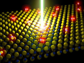 |
| This is a schematic of a laser beam energizing a monolayer semiconductor made up of molybdenum disulfide (MoS2). The red glowing dots are particles excited by the laser.
Image by Der-Hsien Lien |
Abstract:
An emerging class of atomically thin materials known as monolayer semiconductors has generated a great deal of buzz in the world of materials science. Monolayers hold promise in the development of transparent LED displays, ultra-high efficiency solar cells, photo detectors and nanoscale transistors. Their downside? The films are notoriously riddled with defects, killing their performance.
Coming to a monitor near you: A defect-free, molecule-thick film
Berkeley, CA | Posted on November 29th, 2015But now a research team, led by engineers at the University of California, Berkeley, and Lawrence Berkeley National Laboratory, has found a simple way to fix these defects through the use of an organic superacid. The chemical treatment led to a dramatic 100-fold increase in the material's photoluminescence quantum yield, a ratio describing the amount of light generated by the material versus the amount of energy put in. The greater the emission of light, the higher the quantum yield and the better the material quality.
The researchers enhanced the quantum yield for molybdenum disulfide, or MoS2, from less than 1 percent up to 100 percent by dipping the material into a superacid called bistriflimide, or TFSI.
Their findings, to be published in the Nov. 27 issue of Science, opens the door to the practical application of monolayer materials, such as MoS2, in optoelectronic devices and high-performance transistors. MoS2 is a mere seven-tenths of a nanometer thick. For comparison, a strand of human DNA is 2.5 nanometers in diameter.
"Traditionally, the thinner the material, the more sensitive it is to defects," said principal investigator Ali Javey, UC Berkeley professor of electrical engineering and computer sciences and a faculty scientist at Berkeley Lab. "This study presents the first demonstration of an optoelectronically perfect monolayer, which previously had been unheard of in a material this thin."
The researchers looked to superacids because, by definition, they are solutions with a propensity to "give" protons, often in the form of hydrogen atoms, to other substances. This chemical reaction, called protonation, has the effect of filling in for the missing atoms at the site of defects as well as removing unwanted contaminants stuck on the surface, the researchers said.
Co-lead authors of the paper are UC Berkeley Ph.D. student Matin Amani, visiting Ph.D. student Der-Hsien Lien and postdoctoral fellow Daisuke Kiriya.
They noted that scientists have been pursuing monolayer semiconductors because of their low absorption of light and their ability to withstand twists, bends and other extreme forms of mechanical deformation, which can enable their use in transparent or flexible devices.
MoS2, specifically, is characterized by molecular layers held together by van der Waals forces, a type of atomic bonding between each layer that is atomically sharp. An added benefit of having a material that is so thin is that it is highly electrically tunable. For applications such as LED displays, this feature may allow devices to be made where a single pixel could emit a wide range of colors rather than just one by varying the amount of voltage applied.
The lead authors added that the efficiency of an LED is directly related to the photoluminescence quantum yield so, in principle, one could develop high-performance LED displays that are transparent when powered off and flexible using the "perfect" optoelectronic monolayers produced in this study.
This treatment also has revolutionary potential for transistors. As devices in computer chips get smaller and thinner, defects play a bigger role in limiting their performance.
"The defect-free monolayers developed here could solve this problem in addition to allowing for new types of low-energy switches," said Javey.
###
Xiang Zhang and Eli Yablonovitch, faculty members with joint appointments at UC Berkeley's College of Engineering and Berkeley Lab, co-authored this paper. Other co-authors include researchers from National Taiwan University, the University of Texas and the U.S. Army Research Laboratory in Maryland.
The work was funded by the U.S. Department of Energy, the National Science Foundation Center for Energy Efficient Electronics and Science at UC Berkeley, Samsung and the Center for Low Energy System Technology.
####
For more information, please click here
Contacts:
Sarah Yang
510-643-7741
Copyright © University of California, Berkeley
If you have a comment, please Contact us.Issuers of news releases, not 7th Wave, Inc. or Nanotechnology Now, are solely responsible for the accuracy of the content.
Bookmark:


| Related News Press |
News and information
![]() Quantum computer improves AI predictions April 17th, 2026
Quantum computer improves AI predictions April 17th, 2026
![]() Flexible sensor gains sensitivity under pressure April 17th, 2026
Flexible sensor gains sensitivity under pressure April 17th, 2026
![]() A reusable chip for particulate matter sensing April 17th, 2026
A reusable chip for particulate matter sensing April 17th, 2026
![]() Detecting vibrational quantum beating in the predissociation dynamics of SF6 using time-resolved photoelectron spectroscopy April 17th, 2026
Detecting vibrational quantum beating in the predissociation dynamics of SF6 using time-resolved photoelectron spectroscopy April 17th, 2026
Display technology/LEDs/SS Lighting/OLEDs
![]() Spinel-type sulfide semiconductors to operate the next-generation LEDs and solar cells For solar-cell absorbers and green-LED source October 3rd, 2025
Spinel-type sulfide semiconductors to operate the next-generation LEDs and solar cells For solar-cell absorbers and green-LED source October 3rd, 2025
Laboratories
![]() Researchers develop molecular qubits that communicate at telecom frequencies October 3rd, 2025
Researchers develop molecular qubits that communicate at telecom frequencies October 3rd, 2025
Govt.-Legislation/Regulation/Funding/Policy
![]() Quantum computer improves AI predictions April 17th, 2026
Quantum computer improves AI predictions April 17th, 2026
![]() Metasurfaces smooth light to boost magnetic sensing precision January 30th, 2026
Metasurfaces smooth light to boost magnetic sensing precision January 30th, 2026
![]() New imaging approach transforms study of bacterial biofilms August 8th, 2025
New imaging approach transforms study of bacterial biofilms August 8th, 2025
Chip Technology
![]() A reusable chip for particulate matter sensing April 17th, 2026
A reusable chip for particulate matter sensing April 17th, 2026
![]() Metasurfaces smooth light to boost magnetic sensing precision January 30th, 2026
Metasurfaces smooth light to boost magnetic sensing precision January 30th, 2026
Sensors
![]() Flexible sensor gains sensitivity under pressure April 17th, 2026
Flexible sensor gains sensitivity under pressure April 17th, 2026
![]() Tiny nanosheets, big leap: A new sensor detects ethanol at ultra-low levels January 30th, 2026
Tiny nanosheets, big leap: A new sensor detects ethanol at ultra-low levels January 30th, 2026
![]() From sensors to smart systems: the rise of AI-driven photonic noses January 30th, 2026
From sensors to smart systems: the rise of AI-driven photonic noses January 30th, 2026
![]() Sensors innovations for smart lithium-based batteries: advancements, opportunities, and potential challenges August 8th, 2025
Sensors innovations for smart lithium-based batteries: advancements, opportunities, and potential challenges August 8th, 2025
Discoveries
![]() Quantum computer improves AI predictions April 17th, 2026
Quantum computer improves AI predictions April 17th, 2026
![]() Flexible sensor gains sensitivity under pressure April 17th, 2026
Flexible sensor gains sensitivity under pressure April 17th, 2026
![]() A reusable chip for particulate matter sensing April 17th, 2026
A reusable chip for particulate matter sensing April 17th, 2026
![]() Detecting vibrational quantum beating in the predissociation dynamics of SF6 using time-resolved photoelectron spectroscopy April 17th, 2026
Detecting vibrational quantum beating in the predissociation dynamics of SF6 using time-resolved photoelectron spectroscopy April 17th, 2026
Materials/Metamaterials/Magnetoresistance
![]() First real-time observation of two-dimensional melting process: Researchers at Mainz University unveil new insights into magnetic vortex structures August 8th, 2025
First real-time observation of two-dimensional melting process: Researchers at Mainz University unveil new insights into magnetic vortex structures August 8th, 2025
![]() Researchers unveil a groundbreaking clay-based solution to capture carbon dioxide and combat climate change June 6th, 2025
Researchers unveil a groundbreaking clay-based solution to capture carbon dioxide and combat climate change June 6th, 2025
![]() A 1960s idea inspires NBI researchers to study hitherto inaccessible quantum states June 6th, 2025
A 1960s idea inspires NBI researchers to study hitherto inaccessible quantum states June 6th, 2025
![]() Institute for Nanoscience hosts annual proposal planning meeting May 16th, 2025
Institute for Nanoscience hosts annual proposal planning meeting May 16th, 2025
Announcements
![]() A fundamentally new therapeutic approach to cystic fibrosis: Nanobody repairs cellular defect April 17th, 2026
A fundamentally new therapeutic approach to cystic fibrosis: Nanobody repairs cellular defect April 17th, 2026
![]() UC Irvine physicists discover method to reverse �quantum scrambling� : The work addresses the problem of information loss in quantum computing system April 17th, 2026
UC Irvine physicists discover method to reverse �quantum scrambling� : The work addresses the problem of information loss in quantum computing system April 17th, 2026
Interviews/Book Reviews/Essays/Reports/Podcasts/Journals/White papers/Posters
![]() A fundamentally new therapeutic approach to cystic fibrosis: Nanobody repairs cellular defect April 17th, 2026
A fundamentally new therapeutic approach to cystic fibrosis: Nanobody repairs cellular defect April 17th, 2026
![]() UC Irvine physicists discover method to reverse �quantum scrambling� : The work addresses the problem of information loss in quantum computing system April 17th, 2026
UC Irvine physicists discover method to reverse �quantum scrambling� : The work addresses the problem of information loss in quantum computing system April 17th, 2026
Energy
![]() Sensors innovations for smart lithium-based batteries: advancements, opportunities, and potential challenges August 8th, 2025
Sensors innovations for smart lithium-based batteries: advancements, opportunities, and potential challenges August 8th, 2025
![]() Simple algorithm paired with standard imaging tool could predict failure in lithium metal batteries August 8th, 2025
Simple algorithm paired with standard imaging tool could predict failure in lithium metal batteries August 8th, 2025
Grants/Sponsored Research/Awards/Scholarships/Gifts/Contests/Honors/Records
![]() Quantum computer improves AI predictions April 17th, 2026
Quantum computer improves AI predictions April 17th, 2026
![]() Detecting vibrational quantum beating in the predissociation dynamics of SF6 using time-resolved photoelectron spectroscopy April 17th, 2026
Detecting vibrational quantum beating in the predissociation dynamics of SF6 using time-resolved photoelectron spectroscopy April 17th, 2026
![]() Metasurfaces smooth light to boost magnetic sensing precision January 30th, 2026
Metasurfaces smooth light to boost magnetic sensing precision January 30th, 2026
Research partnerships
![]() Lab to industry: InSe wafer-scale breakthrough for future electronics August 8th, 2025
Lab to industry: InSe wafer-scale breakthrough for future electronics August 8th, 2025
![]() HKU physicists uncover hidden order in the quantum world through deconfined quantum critical points April 25th, 2025
HKU physicists uncover hidden order in the quantum world through deconfined quantum critical points April 25th, 2025
Solar/Photovoltaic
![]() Spinel-type sulfide semiconductors to operate the next-generation LEDs and solar cells For solar-cell absorbers and green-LED source October 3rd, 2025
Spinel-type sulfide semiconductors to operate the next-generation LEDs and solar cells For solar-cell absorbers and green-LED source October 3rd, 2025
![]() KAIST researchers introduce new and improved, next-generation perovskite solar cell November 8th, 2024
KAIST researchers introduce new and improved, next-generation perovskite solar cell November 8th, 2024
![]() Groundbreaking precision in single-molecule optoelectronics August 16th, 2024
Groundbreaking precision in single-molecule optoelectronics August 16th, 2024
![]() Development of zinc oxide nanopagoda array photoelectrode: photoelectrochemical water-splitting hydrogen production January 12th, 2024
Development of zinc oxide nanopagoda array photoelectrode: photoelectrochemical water-splitting hydrogen production January 12th, 2024
|
|
||
|
|
||
| The latest news from around the world, FREE | ||
|
|
||
|
|
||
| Premium Products | ||
|
|
||
|
Only the news you want to read!
Learn More |
||
|
|
||
|
Full-service, expert consulting
Learn More |
||
|
|
||