Home > Press > Manipulating wrinkles could lead to graphene semiconductors
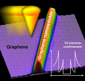 |
| Schematic of the work The tip of the scanning tunneling microscope (in yellow-orange) is moved over the graphene and the nanowrinkle. |
Abstract:
Graphene has generally been described as a two-dimensional structure--a single sheet of carbon atoms arranged in a regular structure--but the reality is not so simple. In reality, graphene can form wrinkles which make the structure more complicated, potentially being applied to device systems. The graphene can also interact with the substrate upon which it is laid, adding further complexity. In research published in Nature Communications, RIKEN scientists have now discovered that wrinkles in graphene can restrict the motion of electrons to one dimension, forming a junction-like structure that changes from zero-gap conductor to semiconductor back to zero-gap conductor. Moreover, they have used the tip of a scanning tunneling microscope to manipulate the formation of wrinkles, opening the way to the construction of graphene semiconductors not through chemical means--by adding other elements--but by manipulating the carbon structure itself in a form of "graphene engineering."
Manipulating wrinkles could lead to graphene semiconductors
Wako, Japan | Posted on October 23rd, 2015The discovery began when the group was experimenting with creating graphene films using chemical vapor deposition, which is considered the most reliable method. They were working to form graphene on a nickel substrate, but the success of this method depends heavily on the temperature and cooling speed.
According to Hyunseob Lim, the first author of the paper, "We were attempting to grow graphene on a single crystalline nickel substrate, but in many cases we ended up creating a compound of nickel and carbon, Ni2C, rather than graphene. In order to resolve the problem, we tried quickly cooling the sample after the dosing with acetylene, and during that process we accidentally found small nanowrinkles, just five nanometers wide, in the sample."
They were able to image these tiny wrinkles using scanning tunneling microscopy, and discovered that there were band gap openings within them, indicating that the wrinkles could act as semiconductors. Normally electrons and electron holes flow freely through a conductor without a band gap, but when it is a semiconductor there are band gaps between the permitted electron states, and the electrons can only pass through these gaps under certain conditions. This indicates that the graphene could, depending on the wrinkles, become a semiconductor.
Initially they considered two possibilities for the emergence of this band gap. One is that the mechanical strain could cause a magnetic phenomenon, but they ruled this out, and concluded that the phenomenon was caused by the confinement of electrons in a single dimension due to "quantum confinement."
According to Yousoo Kim, head of the Surface and Interface Science Laboratory, who led the team, "Up until now, efforts to manipulate the electronic properties of graphene have principally been done through chemical means, but the downside of this is that it can lead to degraded electronic properties due to chemical defects. Here we have shown that the electronic properties can be manipulated merely by changing the shape of the carbon structure. It will be exciting to see if this could lead to ways to find new uses for graphene."
####
For more information, please click here
Contacts:
Jens Wilkinson
81-484-621-225
Copyright © RIKEN
If you have a comment, please Contact us.Issuers of news releases, not 7th Wave, Inc. or Nanotechnology Now, are solely responsible for the accuracy of the content.
Bookmark:


| Related News Press |
News and information
![]() Quantum computer improves AI predictions April 17th, 2026
Quantum computer improves AI predictions April 17th, 2026
![]() Flexible sensor gains sensitivity under pressure April 17th, 2026
Flexible sensor gains sensitivity under pressure April 17th, 2026
![]() A reusable chip for particulate matter sensing April 17th, 2026
A reusable chip for particulate matter sensing April 17th, 2026
![]() Detecting vibrational quantum beating in the predissociation dynamics of SF6 using time-resolved photoelectron spectroscopy April 17th, 2026
Detecting vibrational quantum beating in the predissociation dynamics of SF6 using time-resolved photoelectron spectroscopy April 17th, 2026
Graphene/ Graphite
![]() Electrifying results shed light on graphene foam as a potential material for lab grown cartilage June 6th, 2025
Electrifying results shed light on graphene foam as a potential material for lab grown cartilage June 6th, 2025
![]() Breakthrough in proton barrier films using pore-free graphene oxide: Kumamoto University researchers achieve new milestone in advanced coating technologies September 13th, 2024
Breakthrough in proton barrier films using pore-free graphene oxide: Kumamoto University researchers achieve new milestone in advanced coating technologies September 13th, 2024
Chip Technology
![]() A reusable chip for particulate matter sensing April 17th, 2026
A reusable chip for particulate matter sensing April 17th, 2026
![]() Metasurfaces smooth light to boost magnetic sensing precision January 30th, 2026
Metasurfaces smooth light to boost magnetic sensing precision January 30th, 2026
Nanoelectronics
![]() Lab to industry: InSe wafer-scale breakthrough for future electronics August 8th, 2025
Lab to industry: InSe wafer-scale breakthrough for future electronics August 8th, 2025
![]() Interdisciplinary: Rice team tackles the future of semiconductors Multiferroics could be the key to ultralow-energy computing October 6th, 2023
Interdisciplinary: Rice team tackles the future of semiconductors Multiferroics could be the key to ultralow-energy computing October 6th, 2023
![]() Key element for a scalable quantum computer: Physicists from Forschungszentrum J�lich and RWTH Aachen University demonstrate electron transport on a quantum chip September 23rd, 2022
Key element for a scalable quantum computer: Physicists from Forschungszentrum J�lich and RWTH Aachen University demonstrate electron transport on a quantum chip September 23rd, 2022
![]() Reduced power consumption in semiconductor devices September 23rd, 2022
Reduced power consumption in semiconductor devices September 23rd, 2022
Discoveries
![]() Quantum computer improves AI predictions April 17th, 2026
Quantum computer improves AI predictions April 17th, 2026
![]() Flexible sensor gains sensitivity under pressure April 17th, 2026
Flexible sensor gains sensitivity under pressure April 17th, 2026
![]() A reusable chip for particulate matter sensing April 17th, 2026
A reusable chip for particulate matter sensing April 17th, 2026
![]() Detecting vibrational quantum beating in the predissociation dynamics of SF6 using time-resolved photoelectron spectroscopy April 17th, 2026
Detecting vibrational quantum beating in the predissociation dynamics of SF6 using time-resolved photoelectron spectroscopy April 17th, 2026
Announcements
![]() A fundamentally new therapeutic approach to cystic fibrosis: Nanobody repairs cellular defect April 17th, 2026
A fundamentally new therapeutic approach to cystic fibrosis: Nanobody repairs cellular defect April 17th, 2026
![]() UC Irvine physicists discover method to reverse �quantum scrambling� : The work addresses the problem of information loss in quantum computing system April 17th, 2026
UC Irvine physicists discover method to reverse �quantum scrambling� : The work addresses the problem of information loss in quantum computing system April 17th, 2026
Interviews/Book Reviews/Essays/Reports/Podcasts/Journals/White papers/Posters
![]() A fundamentally new therapeutic approach to cystic fibrosis: Nanobody repairs cellular defect April 17th, 2026
A fundamentally new therapeutic approach to cystic fibrosis: Nanobody repairs cellular defect April 17th, 2026
![]() UC Irvine physicists discover method to reverse �quantum scrambling� : The work addresses the problem of information loss in quantum computing system April 17th, 2026
UC Irvine physicists discover method to reverse �quantum scrambling� : The work addresses the problem of information loss in quantum computing system April 17th, 2026
Quantum nanoscience
![]() Beyond silicon: Electronics at the scale of a single molecule January 30th, 2026
Beyond silicon: Electronics at the scale of a single molecule January 30th, 2026
![]() MXene nanomaterials enter a new dimension Multilayer nanomaterial: MXene flakes created at Drexel University show new promise as 1D scrolls January 30th, 2026
MXene nanomaterials enter a new dimension Multilayer nanomaterial: MXene flakes created at Drexel University show new promise as 1D scrolls January 30th, 2026
![]() ICFO researchers overcome long-standing bottleneck in single photon detection with twisted 2D materials August 8th, 2025
ICFO researchers overcome long-standing bottleneck in single photon detection with twisted 2D materials August 8th, 2025
|
|
||
|
|
||
| The latest news from around the world, FREE | ||
|
|
||
|
|
||
| Premium Products | ||
|
|
||
|
Only the news you want to read!
Learn More |
||
|
|
||
|
Full-service, expert consulting
Learn More |
||
|
|
||