Home > Press > Thin films offer promise for ferroelectric devices: Researchers at Tokyo Institute of Technology demystify the ferroelectric properties observed in hafnium-oxide-based thin films, revealing a potentially useful device material
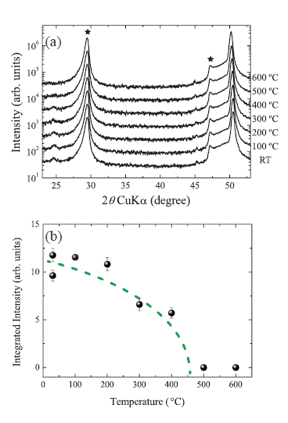 |
| The x-ray diffraction patterns with inclination angle of 45° observed for 0.07YO1.5-0.93HfO2 film measured from room temperature to 600° C. (b) The integrated intensity of the 111 super-spot of 0.07YO1.5-0.93HfO2 film as a function of temperature. |
Abstract:
Ferroelectric materials have applications in next-generation electronics devices from optoelectronic modulators and random access memory to piezoelectric transducers and tunnel junctions. Now researchers at Tokyo Institute of Technology report insights into the properties of epitaxial hafnium-oxide-based (HfO2-based) thin films, confirming a stable ferroelectric phase up to 450 °C. As they point out, “This temperature is sufficiently high for HfO2-based ferroelectric materials to be used in stable device operation and processing as this temperature is comparable to those of other conventional ferroelectric materials.”
Thin films offer promise for ferroelectric devices: Researchers at Tokyo Institute of Technology demystify the ferroelectric properties observed in hafnium-oxide-based thin films, revealing a potentially useful device material
Tokyo, Japan | Posted on August 3rd, 2015Reports of ferroelectric properties in thin films of substituted hafnium-oxide - where some ions were replaced with other metals - have attracted particular interest because these films are already used in electronics and are compatible with the silicon fabrication techniques that dominate the industry. However attempts to study the crystal structure of HfO2-based thin films in detail to understand these ferroelectric properties have met with challenges due to the random orientation of the polycrystalline films.
In order to obtain thin films with a well-defined crystal orientation, Takao Shimizu, Hiroshi Funakubo and colleagues at Tokyo Institute of Technology turned to a growth approach that had not been tried with HfO2-based materials before - epitaxial film growth. They then used a range of characterisation techniques ― including x-ray diffraction analysis and wide-area reciprocal space mapping ― to identify changes in the crystal structure as the yttrium content increased. They found a change from a low- to a high-symmetry phase via an interim orthorhombic phase with increasing yttrium from -15 % substituted yttrium oxide.
Further studies confirmed that this orthorhombic phase is ferroelectric and stable for temperatures up to 450 °C. They conclude, “The present results help to clarify the nature of ferroelectricity in HfO2-based ferroelectric materials and also its potential application in various devices.”
Background
Hafnium oxide thin films
The dielectric constant (high-κ) of HfO2 has previously attracted interest for use in electronics components such as dynamic random-access memory (DRAM) capacitors and is already used for high-κ gates in devices. As a result its compatibility with the CMOS processing that dominates current electronics fabrication is already known.
Ferroelectric properties have been reported in HfO2 thin films with some hafnium ions substituted by different types of ions including yttrium, aluminium and lanthanum, as well as silicon and zirconium. The researchers studied HfO2 films substituted with the yttrium oxide YO1.5 as ferroelectric properties have already been reported in films of this material.
Epitaxial growth
Well-defined crystal orientation with respect to the substrate can be obtained in epitaxially grown films but the process usually requires high temperatures. Due to the tendency to decompose into non-ferroelectric phases HfO2 are usually prepared by crystallization of amorphous films. The researchers used pulsed laser deposition to prepare epitaxially grown HfO2-based films without destroying the ferroelectric phase. The films were grown on yttria-stabilised zirconia and were around 20 nm thick.
Crystal phases and characterization
HfO2 exists in a stable low-symmetry monoclinic phase, where the structure resembles rectangular prism with a parallelogram base. This structure changes to a high-symmetry cubic or tetragonal structured phase through a metastable orthorhombic phase.
Monoclinic, cubic and tetragonal crystalline structures have inversion canter, which rules out ferroelectric properties. Therefore the researchers focused on the orthorhombic. The coexistence of several phases in HfO2 further complicates studies of crystal structure, making it yet more desirable to obtain films with well-defined crystal orientations. Prior to the current work it was still unclear whether epitaxial growth of HfO2-based films was possible.
Previous work had used transmission electron microscopy and simultaneous convergent beam electron diffraction to confirm the existence of the orthorhombic phase, but more detailed analysis of the crystalline structure proved difficult due to the random polycrystalline orientation.
With the epitaxially grown thin films the researchers were able to use x-ray diffraction analysis and wide-area reciprocal space mapping measurements to identify the orthorhombic phase. They then used aberration-corrected annular bright-field and high angle annular dark field scanning transmission electron microscopy to confirm that the orthorhombic phase was ferroelectric.
Reference
Authors: Takao Shimizu, Kiliha Katayama, Takanori Kiguchi, Akihiro Akama, Toyohiko J. Konno and Hiroshi Funakubo
Title: Growth of epitaxial orthorhombic YO1.5-substituted HfO2 thin film
Journal: Applies Physics Letters, Vol 107, page 032910, (2015)
DOI : 10.1063/1.4927450
####
About Tokyo Institute of Technology
As one of Japan’s top universities, Tokyo Institute of Technology seeks to contribute to civilization, peace and prosperity in the world, and aims at developing global human capabilities par excellence through pioneering research and education in science and technology, including industrial and social management. To achieve this mission, we have an eye on educating highly moral students to acquire not only scientific expertise but also expertise in the liberal arts, and a balanced knowledge of the social sciences and humanities, all while researching deeply from basics to practice with academic mastery. Through these activities, we wish to contribute to global sustainability of the natural world and the support of human life.
For more information, please click here
Contacts:
Asuka Suzuki
Center for Public Affairs and Communications, Tokyo Institute of Technology
2-12-1, Ookayama, Meguro-ku, Tokyo 152-8550, Japan
URL: http://www.titech.ac.jp/english/
Tel: +81-3-5734-2975
Fax: +81-3-5734-3661
Copyright © Tokyo Institute of Technology
If you have a comment, please Contact us.Issuers of news releases, not 7th Wave, Inc. or Nanotechnology Now, are solely responsible for the accuracy of the content.
Bookmark:


| Related News Press |
News and information
![]() Quantum computer improves AI predictions April 17th, 2026
Quantum computer improves AI predictions April 17th, 2026
![]() Flexible sensor gains sensitivity under pressure April 17th, 2026
Flexible sensor gains sensitivity under pressure April 17th, 2026
![]() A reusable chip for particulate matter sensing April 17th, 2026
A reusable chip for particulate matter sensing April 17th, 2026
![]() Detecting vibrational quantum beating in the predissociation dynamics of SF6 using time-resolved photoelectron spectroscopy April 17th, 2026
Detecting vibrational quantum beating in the predissociation dynamics of SF6 using time-resolved photoelectron spectroscopy April 17th, 2026
Imaging
![]() Simple algorithm paired with standard imaging tool could predict failure in lithium metal batteries August 8th, 2025
Simple algorithm paired with standard imaging tool could predict failure in lithium metal batteries August 8th, 2025
![]() First real-time observation of two-dimensional melting process: Researchers at Mainz University unveil new insights into magnetic vortex structures August 8th, 2025
First real-time observation of two-dimensional melting process: Researchers at Mainz University unveil new insights into magnetic vortex structures August 8th, 2025
Thin films
![]() Tiny nanosheets, big leap: A new sensor detects ethanol at ultra-low levels January 30th, 2026
Tiny nanosheets, big leap: A new sensor detects ethanol at ultra-low levels January 30th, 2026
Chip Technology
![]() A reusable chip for particulate matter sensing April 17th, 2026
A reusable chip for particulate matter sensing April 17th, 2026
![]() Metasurfaces smooth light to boost magnetic sensing precision January 30th, 2026
Metasurfaces smooth light to boost magnetic sensing precision January 30th, 2026
Discoveries
![]() Quantum computer improves AI predictions April 17th, 2026
Quantum computer improves AI predictions April 17th, 2026
![]() Flexible sensor gains sensitivity under pressure April 17th, 2026
Flexible sensor gains sensitivity under pressure April 17th, 2026
![]() A reusable chip for particulate matter sensing April 17th, 2026
A reusable chip for particulate matter sensing April 17th, 2026
![]() Detecting vibrational quantum beating in the predissociation dynamics of SF6 using time-resolved photoelectron spectroscopy April 17th, 2026
Detecting vibrational quantum beating in the predissociation dynamics of SF6 using time-resolved photoelectron spectroscopy April 17th, 2026
Materials/Metamaterials/Magnetoresistance
![]() First real-time observation of two-dimensional melting process: Researchers at Mainz University unveil new insights into magnetic vortex structures August 8th, 2025
First real-time observation of two-dimensional melting process: Researchers at Mainz University unveil new insights into magnetic vortex structures August 8th, 2025
![]() Researchers unveil a groundbreaking clay-based solution to capture carbon dioxide and combat climate change June 6th, 2025
Researchers unveil a groundbreaking clay-based solution to capture carbon dioxide and combat climate change June 6th, 2025
![]() A 1960s idea inspires NBI researchers to study hitherto inaccessible quantum states June 6th, 2025
A 1960s idea inspires NBI researchers to study hitherto inaccessible quantum states June 6th, 2025
![]() Institute for Nanoscience hosts annual proposal planning meeting May 16th, 2025
Institute for Nanoscience hosts annual proposal planning meeting May 16th, 2025
Announcements
![]() A fundamentally new therapeutic approach to cystic fibrosis: Nanobody repairs cellular defect April 17th, 2026
A fundamentally new therapeutic approach to cystic fibrosis: Nanobody repairs cellular defect April 17th, 2026
![]() UC Irvine physicists discover method to reverse ‘quantum scrambling’ : The work addresses the problem of information loss in quantum computing system April 17th, 2026
UC Irvine physicists discover method to reverse ‘quantum scrambling’ : The work addresses the problem of information loss in quantum computing system April 17th, 2026
Interviews/Book Reviews/Essays/Reports/Podcasts/Journals/White papers/Posters
![]() A fundamentally new therapeutic approach to cystic fibrosis: Nanobody repairs cellular defect April 17th, 2026
A fundamentally new therapeutic approach to cystic fibrosis: Nanobody repairs cellular defect April 17th, 2026
![]() UC Irvine physicists discover method to reverse ‘quantum scrambling’ : The work addresses the problem of information loss in quantum computing system April 17th, 2026
UC Irvine physicists discover method to reverse ‘quantum scrambling’ : The work addresses the problem of information loss in quantum computing system April 17th, 2026
Tools
![]() Metasurfaces smooth light to boost magnetic sensing precision January 30th, 2026
Metasurfaces smooth light to boost magnetic sensing precision January 30th, 2026
![]() From sensors to smart systems: the rise of AI-driven photonic noses January 30th, 2026
From sensors to smart systems: the rise of AI-driven photonic noses January 30th, 2026
![]() Japan launches fully domestically produced quantum computer: Expo visitors to experience quantum computing firsthand August 8th, 2025
Japan launches fully domestically produced quantum computer: Expo visitors to experience quantum computing firsthand August 8th, 2025
Industrial
![]() Tiny nanosheets, big leap: A new sensor detects ethanol at ultra-low levels January 30th, 2026
Tiny nanosheets, big leap: A new sensor detects ethanol at ultra-low levels January 30th, 2026
![]() Quantum interference in molecule-surface collisions February 28th, 2025
Quantum interference in molecule-surface collisions February 28th, 2025
![]() Boron nitride nanotube fibers get real: Rice lab creates first heat-tolerant, stable fibers from wet-spinning process June 24th, 2022
Boron nitride nanotube fibers get real: Rice lab creates first heat-tolerant, stable fibers from wet-spinning process June 24th, 2022
|
|
||
|
|
||
| The latest news from around the world, FREE | ||
|
|
||
|
|
||
| Premium Products | ||
|
|
||
|
Only the news you want to read!
Learn More |
||
|
|
||
|
Full-service, expert consulting
Learn More |
||
|
|
||