Home > Press > Penn researchers discover new chiral property of silicon, with photonic applications
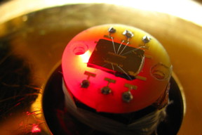 |
| By encoding information in photons via their spin, photonic computers could be orders of magnitude faster and efficient than their current-day counterparts. Likewise, encoding information in the spin of electrons, rather than just their quantity, could make spintronic computers with similar advantages. University of Pennsylvania engineers and physicists have now discovered a property of silicon that combines aspects of all of these desirable qualities. In their experimental set-up, pictured here, they a silicon-based photonic device that is sensitive to the spin of the photons in a laser shined on one of its electrodes. Light that is polarized clockwise causes current to flow in one direction, while counter-clockwise polarized light makes it flow in the other direction. CREDIT: University of Pennsylvania |
Abstract:
By encoding information in photons via their spin, "photonic" computers could be orders of magnitude faster and efficient than their current-day counterparts. Likewise, encoding information in the spin of electrons, rather than just their quantity, could make "spintronic" computers with similar advantages.
Penn researchers discover new chiral property of silicon, with photonic applications
Philadelphia, PA | Posted on July 25th, 2015University of Pennsylvania engineers and physicists have now discovered a property of silicon that combines aspects of all of these desirable qualities.
In a study published in Science, they have demonstrated a silicon-based photonic device that is sensitive to the spin of the photons in a laser shined on one of its electrodes. Light that is polarized clockwise causes current to flow in one direction, while counter-clockwise polarized light makes it flow in the other direction.
This property was hiding in plain sight; it is a function of the geometric relationship between the pattern of atoms on the surface of silicon nanowires and how electrodes placed on those wires intersect them. The interaction between the semiconducting silicon and the metallic electrodes produces an electric field at an angle that breaks the mirror symmetry that silicon typically exhibits. This chiral property is what sends electrons in one direction or the other down the nanowire depending on the polarity of the light that hits the electrodes.
The study was led by Ritesh Agarwal, a professor in the Department of Materials Science and Engineering in Penn's School of Engineering and Applied Science, and Sajal Dhara, a postdoctoral researcher in Agarwal's lab. They collaborated with Eugene Mele, a professor in the Department of Physics and Astronomy in Penn's School of Arts & Sciences.
"Whenever you change a symmetry, you can do new things," said Agarwal. "In this case, we have demonstrated how to make a photodetector sensitive to a photon's spin. All photonic computers need photodetectors, but they currently only use the quantity of photons to encode information. This sensitivity to photon spin would be an extra degree of freedom, meaning you could encode additional information on each photon.
"Typically, materials with heavy elements show this property due to their spins strongly interacting with electron's orbital motion, but we have demonstrated this effect on the surface of silicon, originating only from the electron's orbital motion"
Agarwal and Dhara reached out to Mele due to his work on topological insulators. He, along with fellow Penn physicist Charles Kane, laid the foundation for this new a class of materials, which are electrical insulators on their interiors but conduct electricity on their surfaces.
Agarwal's group was working on various materials that exhibit topological effects, but as a check on their methods, Mele suggested trying their experiments with silicon as well. As a light, highly symmetric material, silicon was not thought to be able to exhibit these properties.
"We expected the control experiment to give a null result, instead we discovered something new about nanomaterials," Mele said.
Silicon is the heart of computer industry, so finding ways of producing these types of effects in that element is preferable to learning how to work with the heavier, rarer elements that naturally exhibit them.
Once it was clear that silicon was capable of having chiral properties, the researchers set out to find out the atomic mechanisms behind it.
"The effect was coming from the surface of the nanowire," Dhara said. "The way most silicon nanowires are grown, the atoms are bound in zigzag chains that go along the surface, not down into the wire."
These zigzag patterns are such that placing a mirror on top of them would produce an image that could be superimposed on the original. This is why silicon is not intrinsically chiral. However, when metal electrodes are placed on the wire in the typical perpendicular fashion, they intersect the direction of the chains at a slight angle.
"When you have any metal and any semiconductor in contact, you'll get an electric field at the interface, and it's this field that is breaking the mirror symmetry in the silicon chains," Dhara said.
Because the direction of the electric field does not exactly match the direction of the zigzag chains, there are angles where the silicon is asymmetric. This means it can exhibit chiral properties. Shining a circularly polarized laser at the point on the nanowire where metal and semiconductor meet produces a current, and the spin of the photons in that laser determines the direction of the current's flow.
Dhara and Agarwal are currently working on ways to get planar silicon to exhibit these properties using the same mechanism.
###
The research was supported by the U.S. Army Research Office, the Department of Energy and the National Science Foundation through Penn's Materials Research Science and Engineering Center.
####
For more information, please click here
Contacts:
Evan Lerner
215-573-6604
Copyright © University of Pennsylvania
If you have a comment, please Contact us.Issuers of news releases, not 7th Wave, Inc. or Nanotechnology Now, are solely responsible for the accuracy of the content.
Bookmark:


| Related News Press |
News and information
![]() Quantum computer improves AI predictions April 17th, 2026
Quantum computer improves AI predictions April 17th, 2026
![]() Flexible sensor gains sensitivity under pressure April 17th, 2026
Flexible sensor gains sensitivity under pressure April 17th, 2026
![]() A reusable chip for particulate matter sensing April 17th, 2026
A reusable chip for particulate matter sensing April 17th, 2026
![]() Detecting vibrational quantum beating in the predissociation dynamics of SF6 using time-resolved photoelectron spectroscopy April 17th, 2026
Detecting vibrational quantum beating in the predissociation dynamics of SF6 using time-resolved photoelectron spectroscopy April 17th, 2026
Govt.-Legislation/Regulation/Funding/Policy
![]() Quantum computer improves AI predictions April 17th, 2026
Quantum computer improves AI predictions April 17th, 2026
![]() Metasurfaces smooth light to boost magnetic sensing precision January 30th, 2026
Metasurfaces smooth light to boost magnetic sensing precision January 30th, 2026
![]() New imaging approach transforms study of bacterial biofilms August 8th, 2025
New imaging approach transforms study of bacterial biofilms August 8th, 2025
Spintronics
![]() Quantum materials: Electron spin measured for the first time June 9th, 2023
Quantum materials: Electron spin measured for the first time June 9th, 2023
Chip Technology
![]() A reusable chip for particulate matter sensing April 17th, 2026
A reusable chip for particulate matter sensing April 17th, 2026
![]() Metasurfaces smooth light to boost magnetic sensing precision January 30th, 2026
Metasurfaces smooth light to boost magnetic sensing precision January 30th, 2026
Optical computing/Photonic computing
![]() ICFO researchers overcome long-standing bottleneck in single photon detection with twisted 2D materials August 8th, 2025
ICFO researchers overcome long-standing bottleneck in single photon detection with twisted 2D materials August 8th, 2025
![]() Programmable electron-induced color router array May 14th, 2025
Programmable electron-induced color router array May 14th, 2025
Discoveries
![]() Quantum computer improves AI predictions April 17th, 2026
Quantum computer improves AI predictions April 17th, 2026
![]() Flexible sensor gains sensitivity under pressure April 17th, 2026
Flexible sensor gains sensitivity under pressure April 17th, 2026
![]() A reusable chip for particulate matter sensing April 17th, 2026
A reusable chip for particulate matter sensing April 17th, 2026
![]() Detecting vibrational quantum beating in the predissociation dynamics of SF6 using time-resolved photoelectron spectroscopy April 17th, 2026
Detecting vibrational quantum beating in the predissociation dynamics of SF6 using time-resolved photoelectron spectroscopy April 17th, 2026
Announcements
![]() A fundamentally new therapeutic approach to cystic fibrosis: Nanobody repairs cellular defect April 17th, 2026
A fundamentally new therapeutic approach to cystic fibrosis: Nanobody repairs cellular defect April 17th, 2026
![]() UC Irvine physicists discover method to reverse �quantum scrambling� : The work addresses the problem of information loss in quantum computing system April 17th, 2026
UC Irvine physicists discover method to reverse �quantum scrambling� : The work addresses the problem of information loss in quantum computing system April 17th, 2026
Interviews/Book Reviews/Essays/Reports/Podcasts/Journals/White papers/Posters
![]() A fundamentally new therapeutic approach to cystic fibrosis: Nanobody repairs cellular defect April 17th, 2026
A fundamentally new therapeutic approach to cystic fibrosis: Nanobody repairs cellular defect April 17th, 2026
![]() UC Irvine physicists discover method to reverse �quantum scrambling� : The work addresses the problem of information loss in quantum computing system April 17th, 2026
UC Irvine physicists discover method to reverse �quantum scrambling� : The work addresses the problem of information loss in quantum computing system April 17th, 2026
Military
![]() Quantum engineers �squeeze� laser frequency combs to make more sensitive gas sensors January 17th, 2025
Quantum engineers �squeeze� laser frequency combs to make more sensitive gas sensors January 17th, 2025
![]() Chainmail-like material could be the future of armor: First 2D mechanically interlocked polymer exhibits exceptional flexibility and strength January 17th, 2025
Chainmail-like material could be the future of armor: First 2D mechanically interlocked polymer exhibits exceptional flexibility and strength January 17th, 2025
![]() Single atoms show their true color July 5th, 2024
Single atoms show their true color July 5th, 2024
![]() NRL charters Navy�s quantum inertial navigation path to reduce drift April 5th, 2024
NRL charters Navy�s quantum inertial navigation path to reduce drift April 5th, 2024
Photonics/Optics/Lasers
![]() Metasurfaces smooth light to boost magnetic sensing precision January 30th, 2026
Metasurfaces smooth light to boost magnetic sensing precision January 30th, 2026
![]() From sensors to smart systems: the rise of AI-driven photonic noses January 30th, 2026
From sensors to smart systems: the rise of AI-driven photonic noses January 30th, 2026
|
|
||
|
|
||
| The latest news from around the world, FREE | ||
|
|
||
|
|
||
| Premium Products | ||
|
|
||
|
Only the news you want to read!
Learn More |
||
|
|
||
|
Full-service, expert consulting
Learn More |
||
|
|
||