Home > Press > Graphene gets competition: Layered semiconducting black arsenic phosphorus as an alternative to silicon
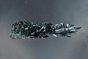 |
| Crystals of black arsenic phosphorus -- exchanging phsphorus against arsenic, the band gap can be tuned to as low as 0.15 eV, making the material predestined for long wavelength infrared sensors. CREDIT: Andreas Battenberg / TUM |
Abstract:
Graphene, the only one atom thick carbon network, achieved overnight fame with the 2010 Nobel Prize. But now comes competition: Such layers can also be formed by black phosphorous. Chemists at the Technische Universität München (TUM) have now developed a semiconducting material in which individual phosphorus atoms are replaced by arsenic. In a collaborative international effort, American colleagues have built the first field-effect transistors from the new material.
Graphene gets competition: Layered semiconducting black arsenic phosphorus as an alternative to silicon
München, Germany | Posted on July 9th, 2015For many decades silicon has formed the basis of modern electronics. To date silicon technology could provide ever tinier transistors for smaller and smaller devices. But the size of silicon transistors is reaching its physical limit. Also, consumers would like to have flexible devices, devices that can be incorporated into clothing and the likes. However, silicon is hard and brittle. All this has triggered a race for new materials that might one day replace silicon.
Black arsenic phosphorus might be such a material. Like graphene, which consists of a single layer of carbon atoms, it forms extremely thin layers. The array of possible applications ranges from transistors and sensors to mechanically flexible semiconductor devices. Unlike graphene, whose electronic properties are similar to those of metals, black arsenic phosphorus behaves like a semiconductor.
Phosphorene vs. graphene
A cooperation between the Technical University of Munich and the University of Regensburg on the German side and the University of Southern California (USC) and Yale University in the United States has now, for the first time, produced a field effect transistor made of black arsenic phosphorus. The compounds were synthesized by Marianne Koepf at the laboratory of the research group for Synthesis and Characterization of Innovative Materials at the TUM. The field effect transistors were built and characterized by a group headed by Professor Zhou and Dr. Liu at the Department of Electrical Engineering at USC.
The new technology developed at TUM allows the synthesis of black arsenic phosphorus without high pressure. This requires less energy and is cheaper. The gap between valence and conduction bands can be precisely controlled by adjusting the arsenic concentration. "This allows us to produce materials with previously unattainable electronic and optical properties in an energy window that was hitherto inaccessible," says Professor Tom Nilges, head of the research group for Synthesis and Characterization of Innovative Materials.
Detectors for infrared
With an arsenic concentration of 83 percent the material exhibits an extremely small band gap of only 0.15 electron volts, making it predestined for sensors which can detect long wavelength infrared radiation. LiDAR (Light Detection and Ranging) sensors operate in this wavelength range, for example. They are used, among other things, as distance sensors in automobiles. Another application is the measurement of dust particles and trace gases in environmental monitoring.
A further interesting aspect of these new, two-dimensional semiconductors is their anisotropic electronic and optical behavior. The material exhibits different characteristics along the x- and y-axes in the same plane. To produce graphene like films the material can be peeled off in ultra thin layers. The thinnest films obtained so far are only two atomic layers thick.
###
This work was supported by the Office of Naval Research (ONR), the Air Force Office of Scientific Research (AFOSR), the Center of Excellence for Nanotechnologies (CEGN) of King Abdul-Aziz City for Science and Technology (KACST), the German Research Council (DFG) and the TUM Graduate School.
Publication:
Black Arsenic-Phosphorus: Layered Anisotropic Infrared Semiconductors with Highly Tunable Compositions and Properties
Bilu Liu, Marianne Köpf, Ahmad N. Abbas, Xiaomu Wang, Qiushi Guo, Yichen Jia, Fengnian Xia, Richard Weihrich, Frederik Bachhuber, Florian Pielnhofer, Han Wang, Rohan
Dhall, Stephen B. Cronin, Mingyuan Ge, Xin Fang, Tom Nilges, Chongwu Zhou
Adv. Mater., 2015, Early View - DOI: 10.1002/adma.201501758
####
For more information, please click here
Contacts:
Dr. Andreas Battenberg
49-892-891-0510
Copyright © Technische Universität München
If you have a comment, please Contact us.Issuers of news releases, not 7th Wave, Inc. or Nanotechnology Now, are solely responsible for the accuracy of the content.
Bookmark:


| Related News Press |
News and information
![]() Quantum computer improves AI predictions April 17th, 2026
Quantum computer improves AI predictions April 17th, 2026
![]() Flexible sensor gains sensitivity under pressure April 17th, 2026
Flexible sensor gains sensitivity under pressure April 17th, 2026
![]() A reusable chip for particulate matter sensing April 17th, 2026
A reusable chip for particulate matter sensing April 17th, 2026
![]() Detecting vibrational quantum beating in the predissociation dynamics of SF6 using time-resolved photoelectron spectroscopy April 17th, 2026
Detecting vibrational quantum beating in the predissociation dynamics of SF6 using time-resolved photoelectron spectroscopy April 17th, 2026
Thin films
![]() Tiny nanosheets, big leap: A new sensor detects ethanol at ultra-low levels January 30th, 2026
Tiny nanosheets, big leap: A new sensor detects ethanol at ultra-low levels January 30th, 2026
![]() Utilizing palladium for addressing contact issues of buried oxide thin film transistors April 5th, 2024
Utilizing palladium for addressing contact issues of buried oxide thin film transistors April 5th, 2024
![]() Understanding the mechanism of non-uniform formation of diamond film on tools: Paving the way to a dry process with less environmental impact March 24th, 2023
Understanding the mechanism of non-uniform formation of diamond film on tools: Paving the way to a dry process with less environmental impact March 24th, 2023
![]() New study introduces the best graphite films: The work by Distinguished Professor Feng Ding at UNIST has been published in the October 2022 issue of Nature Nanotechnology November 4th, 2022
New study introduces the best graphite films: The work by Distinguished Professor Feng Ding at UNIST has been published in the October 2022 issue of Nature Nanotechnology November 4th, 2022
Govt.-Legislation/Regulation/Funding/Policy
![]() Quantum computer improves AI predictions April 17th, 2026
Quantum computer improves AI predictions April 17th, 2026
![]() Metasurfaces smooth light to boost magnetic sensing precision January 30th, 2026
Metasurfaces smooth light to boost magnetic sensing precision January 30th, 2026
![]() New imaging approach transforms study of bacterial biofilms August 8th, 2025
New imaging approach transforms study of bacterial biofilms August 8th, 2025
Chip Technology
![]() A reusable chip for particulate matter sensing April 17th, 2026
A reusable chip for particulate matter sensing April 17th, 2026
![]() Metasurfaces smooth light to boost magnetic sensing precision January 30th, 2026
Metasurfaces smooth light to boost magnetic sensing precision January 30th, 2026
Sensors
![]() Flexible sensor gains sensitivity under pressure April 17th, 2026
Flexible sensor gains sensitivity under pressure April 17th, 2026
![]() Tiny nanosheets, big leap: A new sensor detects ethanol at ultra-low levels January 30th, 2026
Tiny nanosheets, big leap: A new sensor detects ethanol at ultra-low levels January 30th, 2026
![]() From sensors to smart systems: the rise of AI-driven photonic noses January 30th, 2026
From sensors to smart systems: the rise of AI-driven photonic noses January 30th, 2026
![]() Sensors innovations for smart lithium-based batteries: advancements, opportunities, and potential challenges August 8th, 2025
Sensors innovations for smart lithium-based batteries: advancements, opportunities, and potential challenges August 8th, 2025
Discoveries
![]() Quantum computer improves AI predictions April 17th, 2026
Quantum computer improves AI predictions April 17th, 2026
![]() Flexible sensor gains sensitivity under pressure April 17th, 2026
Flexible sensor gains sensitivity under pressure April 17th, 2026
![]() A reusable chip for particulate matter sensing April 17th, 2026
A reusable chip for particulate matter sensing April 17th, 2026
![]() Detecting vibrational quantum beating in the predissociation dynamics of SF6 using time-resolved photoelectron spectroscopy April 17th, 2026
Detecting vibrational quantum beating in the predissociation dynamics of SF6 using time-resolved photoelectron spectroscopy April 17th, 2026
Materials/Metamaterials/Magnetoresistance
![]() First real-time observation of two-dimensional melting process: Researchers at Mainz University unveil new insights into magnetic vortex structures August 8th, 2025
First real-time observation of two-dimensional melting process: Researchers at Mainz University unveil new insights into magnetic vortex structures August 8th, 2025
![]() Researchers unveil a groundbreaking clay-based solution to capture carbon dioxide and combat climate change June 6th, 2025
Researchers unveil a groundbreaking clay-based solution to capture carbon dioxide and combat climate change June 6th, 2025
![]() A 1960s idea inspires NBI researchers to study hitherto inaccessible quantum states June 6th, 2025
A 1960s idea inspires NBI researchers to study hitherto inaccessible quantum states June 6th, 2025
![]() Institute for Nanoscience hosts annual proposal planning meeting May 16th, 2025
Institute for Nanoscience hosts annual proposal planning meeting May 16th, 2025
Announcements
![]() A fundamentally new therapeutic approach to cystic fibrosis: Nanobody repairs cellular defect April 17th, 2026
A fundamentally new therapeutic approach to cystic fibrosis: Nanobody repairs cellular defect April 17th, 2026
![]() UC Irvine physicists discover method to reverse ‘quantum scrambling’ : The work addresses the problem of information loss in quantum computing system April 17th, 2026
UC Irvine physicists discover method to reverse ‘quantum scrambling’ : The work addresses the problem of information loss in quantum computing system April 17th, 2026
Interviews/Book Reviews/Essays/Reports/Podcasts/Journals/White papers/Posters
![]() A fundamentally new therapeutic approach to cystic fibrosis: Nanobody repairs cellular defect April 17th, 2026
A fundamentally new therapeutic approach to cystic fibrosis: Nanobody repairs cellular defect April 17th, 2026
![]() UC Irvine physicists discover method to reverse ‘quantum scrambling’ : The work addresses the problem of information loss in quantum computing system April 17th, 2026
UC Irvine physicists discover method to reverse ‘quantum scrambling’ : The work addresses the problem of information loss in quantum computing system April 17th, 2026
Military
![]() Quantum engineers ‘squeeze’ laser frequency combs to make more sensitive gas sensors January 17th, 2025
Quantum engineers ‘squeeze’ laser frequency combs to make more sensitive gas sensors January 17th, 2025
![]() Chainmail-like material could be the future of armor: First 2D mechanically interlocked polymer exhibits exceptional flexibility and strength January 17th, 2025
Chainmail-like material could be the future of armor: First 2D mechanically interlocked polymer exhibits exceptional flexibility and strength January 17th, 2025
![]() Single atoms show their true color July 5th, 2024
Single atoms show their true color July 5th, 2024
![]() NRL charters Navy’s quantum inertial navigation path to reduce drift April 5th, 2024
NRL charters Navy’s quantum inertial navigation path to reduce drift April 5th, 2024
|
|
||
|
|
||
| The latest news from around the world, FREE | ||
|
|
||
|
|
||
| Premium Products | ||
|
|
||
|
Only the news you want to read!
Learn More |
||
|
|
||
|
Full-service, expert consulting
Learn More |
||
|
|
||