Home > Press > Filming the film: Scientists observe photographic exposure live at the nanoscale: Advanced method opens up new opportunities for investigation of dynamic processes
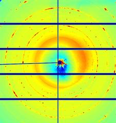 |
| The X-ray diffraction image contains detailed information of the nanostructure of the photosensitive film. Successive images show the dynamic changes during exposure by hiking and splitting individual Diffraktionspunkte. Picture: Jeff (Zhifeng) Huang / UCLA |
Abstract:
Photoinduced chemical reactions are responsible for many fundamental processes and technologies, from energy conversion in nature to micro fabrication by photo-lithography. One process that is known from everyday's life and can be observed by the naked eye, is the exposure of photographic film. At DESY's X-ray light source PETRA III, scientists have now monitored the chemical processes during a photographic exposure at the level of individual nanoscale grains in real-time. The advanced experimental method enables the investigation of a broad variety of chemical and physical processes in materials with millisecond temporal resolution, ranging from phase transitions to crystal growth. The research team lead by Prof. Jianwei (John) Miao from the University of California in Los Angeles and Prof. Tim Salditt from the University of Göttingen report their technique and observations in the journal Nature Materials.
Filming the film: Scientists observe photographic exposure live at the nanoscale: Advanced method opens up new opportunities for investigation of dynamic processes
Hamburg, Germany | Posted on June 9th, 2015The researchers investigated a photographic paper (Kodak linagraph paper Type 2167 or "yellow burn paper") that is often used to determine the position of the beam at X-ray experiments. "The photographic paper we looked at is not specially designed for X-rays. It works by changing its colour on exposure to light or X-rays," explains DESY physicist Dr. Michael Sprung, head of the PETRA III beamline P10 where the experiments took place.
The X-rays were not only used to expose the photographic paper, but also to analyse changes of its inner composition at the same time. The paper carries a photosensitive film of a few micrometre thickness, consisting of tiny silver bromide grains dispersed in a gelatine matrix, and with an average size of about 700 nanometres. A nanometre is a millionth of a millimetre. When X-rays impinge onto such a crystalline grain, they are diffracted in a characteristic way, forming a unique pattern on the detector that reveals properties like crystal lattice spacing, chemical composition and orientation. "We could observe individual silver bromide grains within the 'burn' paper since the X-ray beam had a size of only 270 by 370 nanometres - smaller than the average grain," says Salditt, who is a partner of DESY in the construction and operation of the GINIX (Göttingen Instrument for Nano-Imaging with X-Rays) at beamline P10.
The X-ray exposure starts the photolysis from silver bromide to produce silver. An absorbed X-ray photon can create many photolytic silver atoms, which grow and agglomerate at the surface and inside the silver bromide grain. The scientists observed how the silver bromide grains were strained, began to turn in the gelatine matrix and broke up into smaller crystallites as well as the growth of pure silver nano grains. The exceptionally bright beam of PETRA III together with a high-speed detector enabled the 'filming' of the process with up to five milliseconds temporal resolution. "We observed, for the first time, grain rotation and lattice deformation during photoinduced chemical reactions," emphasises Miao. "We were actually surprised how fast some of these single grains rotate," adds Sprung. "Some spin almost one time every two seconds."
"As advanced synchrotron light sources are currently under rapid development in the US, Europe and Asia," the authors anticipate that "in situ X-ray nanodiffraction, which enables to measure atomic resolution diffraction patterns with several millisecond temporal resolution, can be broadly applied to investigate phase transitions, chemical reactions, crystal growth, grain boundary dynamics, lattice expansion, and contraction in materials science, nanoscience, physics, and chemistry."
####
About Deutsches Elektronen-Synchrotron DESY
Deutsches Elektronen-Synchrotron DESY is the leading German accelerator centre and one of the leading in the world. DESY is a member of the Helmholtz Association and receives its funding from the German Federal Ministry of Education and Research (BMBF) (90 per cent) and the German federal states of Hamburg and Brandenburg (10 per cent). At its locations in Hamburg and Zeuthen near Berlin, DESY develops, builds and operates large particle accelerators, and uses them to investigate the structure of matter. DESY's combination of photon science and particle physics is unique in Europe.
For more information, please click here
Contacts:
Dr. Thomas Zoufal
49-408-998-1666
Copyright © Deutsches Elektronen-Synchrotron DESY
If you have a comment, please Contact us.Issuers of news releases, not 7th Wave, Inc. or Nanotechnology Now, are solely responsible for the accuracy of the content.
Bookmark:


| Related Links |
| Related News Press |
News and information
![]() Quantum computer improves AI predictions April 17th, 2026
Quantum computer improves AI predictions April 17th, 2026
![]() Flexible sensor gains sensitivity under pressure April 17th, 2026
Flexible sensor gains sensitivity under pressure April 17th, 2026
![]() A reusable chip for particulate matter sensing April 17th, 2026
A reusable chip for particulate matter sensing April 17th, 2026
![]() Detecting vibrational quantum beating in the predissociation dynamics of SF6 using time-resolved photoelectron spectroscopy April 17th, 2026
Detecting vibrational quantum beating in the predissociation dynamics of SF6 using time-resolved photoelectron spectroscopy April 17th, 2026
Imaging
![]() Simple algorithm paired with standard imaging tool could predict failure in lithium metal batteries August 8th, 2025
Simple algorithm paired with standard imaging tool could predict failure in lithium metal batteries August 8th, 2025
Govt.-Legislation/Regulation/Funding/Policy
![]() Quantum computer improves AI predictions April 17th, 2026
Quantum computer improves AI predictions April 17th, 2026
![]() Metasurfaces smooth light to boost magnetic sensing precision January 30th, 2026
Metasurfaces smooth light to boost magnetic sensing precision January 30th, 2026
![]() New imaging approach transforms study of bacterial biofilms August 8th, 2025
New imaging approach transforms study of bacterial biofilms August 8th, 2025
Discoveries
![]() Quantum computer improves AI predictions April 17th, 2026
Quantum computer improves AI predictions April 17th, 2026
![]() Flexible sensor gains sensitivity under pressure April 17th, 2026
Flexible sensor gains sensitivity under pressure April 17th, 2026
![]() A reusable chip for particulate matter sensing April 17th, 2026
A reusable chip for particulate matter sensing April 17th, 2026
![]() Detecting vibrational quantum beating in the predissociation dynamics of SF6 using time-resolved photoelectron spectroscopy April 17th, 2026
Detecting vibrational quantum beating in the predissociation dynamics of SF6 using time-resolved photoelectron spectroscopy April 17th, 2026
Announcements
![]() A fundamentally new therapeutic approach to cystic fibrosis: Nanobody repairs cellular defect April 17th, 2026
A fundamentally new therapeutic approach to cystic fibrosis: Nanobody repairs cellular defect April 17th, 2026
![]() UC Irvine physicists discover method to reverse ‘quantum scrambling’ : The work addresses the problem of information loss in quantum computing system April 17th, 2026
UC Irvine physicists discover method to reverse ‘quantum scrambling’ : The work addresses the problem of information loss in quantum computing system April 17th, 2026
Interviews/Book Reviews/Essays/Reports/Podcasts/Journals/White papers/Posters
![]() A fundamentally new therapeutic approach to cystic fibrosis: Nanobody repairs cellular defect April 17th, 2026
A fundamentally new therapeutic approach to cystic fibrosis: Nanobody repairs cellular defect April 17th, 2026
![]() UC Irvine physicists discover method to reverse ‘quantum scrambling’ : The work addresses the problem of information loss in quantum computing system April 17th, 2026
UC Irvine physicists discover method to reverse ‘quantum scrambling’ : The work addresses the problem of information loss in quantum computing system April 17th, 2026
Tools
![]() Metasurfaces smooth light to boost magnetic sensing precision January 30th, 2026
Metasurfaces smooth light to boost magnetic sensing precision January 30th, 2026
![]() From sensors to smart systems: the rise of AI-driven photonic noses January 30th, 2026
From sensors to smart systems: the rise of AI-driven photonic noses January 30th, 2026
![]() Japan launches fully domestically produced quantum computer: Expo visitors to experience quantum computing firsthand August 8th, 2025
Japan launches fully domestically produced quantum computer: Expo visitors to experience quantum computing firsthand August 8th, 2025
Research partnerships
![]() Lab to industry: InSe wafer-scale breakthrough for future electronics August 8th, 2025
Lab to industry: InSe wafer-scale breakthrough for future electronics August 8th, 2025
![]() HKU physicists uncover hidden order in the quantum world through deconfined quantum critical points April 25th, 2025
HKU physicists uncover hidden order in the quantum world through deconfined quantum critical points April 25th, 2025
Printing/Lithography/Inkjet/Inks/Bio-printing/Dyes
![]() Presenting: Ultrasound-based printing of 3D materials—potentially inside the body December 8th, 2023
Presenting: Ultrasound-based printing of 3D materials—potentially inside the body December 8th, 2023
![]() Simple ballpoint pen can write custom LEDs August 11th, 2023
Simple ballpoint pen can write custom LEDs August 11th, 2023
![]() Disposable electronics on a simple sheet of paper October 7th, 2022
Disposable electronics on a simple sheet of paper October 7th, 2022
|
|
||
|
|
||
| The latest news from around the world, FREE | ||
|
|
||
|
|
||
| Premium Products | ||
|
|
||
|
Only the news you want to read!
Learn More |
||
|
|
||
|
Full-service, expert consulting
Learn More |
||
|
|
||