Home > Press > Combined effort for structural determination
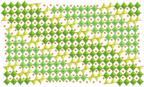 |
| This is the refined structure of (Pb,Bi)1 - xFe1 + xO3 - y. CREDIT: Batuk et al. |
Abstract:
Combining powder diffraction data with electron crystallography can give us a clearer view of modulated structures [Batuk et al. (2015). Acta Cryst. B71, 127-143; doi: 10.1107/S2052520615005466]
Combined effort for structural determination
Chester, UK | Posted on April 15th, 2015Electron crystallography has begun to be used routinely for solving otherwise intractable structures. When performed in an aberration-corrected microscope and combined with spectroscopic techniques, it can offer unprecedented detail down to sub-angstrom resolution. "The result of all this progress is that electron crystallography gives answers to more and more questions that used to be the domain of X-ray or neutron diffraction, and is especially useful when the X-ray or neutron experiment needs to be performed on a powder material, which limits the diffraction information available," explains Lukas Palatinus of the Czech Academy of Sciences in Prague in a commentary piece in Acta Crystallographica Section B [Palatinus (2015). Acta Cryst. B71, 125-126; doi: 10.1107/S2052520615005910].
Palatinus points out that when confronted with modulated structures, in which every atomic position is perturbed from one unit cell to the next by a modulation function, the construction of the structure model is much more complicated than for non-modulated materials. While effective techniques have been developed techniques to solve this problem from single crystal diffraction data, for powder diffraction data another approach to get around the problem is needed, which is where the work of Batuk and colleagues comes to the fore.
Batuk and colleagues have now shown how electron crystallography tools can be used to sidestep the limitations of powder diffraction and complement the structure analysis of modulated structures by powder diffraction. "The authors combine the results of their previous research with new results to provide an impressive overview of the available methods and information they can provide," explains Palatinus. The team investigated a series of anion-deficient perovskites to demonstrate proof of principle. In these materials, modulation arises as a consequence of the presence of crystallographic shear planes that have an average periodicity that is not in synchrony with the materials' basic periodicity.
Palatinus also points out that the choice of these materials was good for the given purpose. "These structures exhibit a wide variety of features that complicate the structure analysis of modulated structures from powder patterns," explains Palatinus. "It allowed the authors to illustrate many techniques and applications like the simultaneous imaging of heavy and light elements, atomic resolution chemical mapping or the mapping of the coordination number." Additionally, given the advent of perovskites in recent years as the focus of research into solar panel materials and other semiconductor applications new detailed information about their structures and properties are increasingly important.
"The local crystallographic information acquired using the scanning transmission electron microscopy (STEM)-based methods in combination with the refinement from powder diffraction data can significantly improve the reliability of the crystal structure investigation," Batuk and colleagues report.
Of course, electron crystallography is very unlikely to make X-ray or neutron diffraction redundant any time soon, points out Palatinus, not least because a lot of materials are too short lived under the degrading eye of the electron beam. Moreover, electron techniques generally cannot be applied in situ in chemical reaction environments nor under pressure, instead requiring near vacuum conditions. Nevertheless, he adds that the team "shows convincingly how the electron crystallography methods have grown to a rich source of detailed information on the crystal structures, and it should convince any reader that resorting to these methods may very quickly solve problems that seem intractable by the more traditional approaches." It seems that as with many areas of study, a combined effort, the teamwork between different techniques that can complement each others, is needed to obtain the best results. "The key to success indeed lies in exploiting the complementarity and synergy between various methods," Palatinus says.
####
For more information, please click here
Contacts:
Jonathan Agbenyega
44-124-434-2878
Copyright © International Union of Crystallography
If you have a comment, please Contact us.Issuers of news releases, not 7th Wave, Inc. or Nanotechnology Now, are solely responsible for the accuracy of the content.
Bookmark:


| Related News Press |
News and information
![]() Quantum computer improves AI predictions April 17th, 2026
Quantum computer improves AI predictions April 17th, 2026
![]() Flexible sensor gains sensitivity under pressure April 17th, 2026
Flexible sensor gains sensitivity under pressure April 17th, 2026
![]() A reusable chip for particulate matter sensing April 17th, 2026
A reusable chip for particulate matter sensing April 17th, 2026
![]() Detecting vibrational quantum beating in the predissociation dynamics of SF6 using time-resolved photoelectron spectroscopy April 17th, 2026
Detecting vibrational quantum beating in the predissociation dynamics of SF6 using time-resolved photoelectron spectroscopy April 17th, 2026
Imaging
![]() Simple algorithm paired with standard imaging tool could predict failure in lithium metal batteries August 8th, 2025
Simple algorithm paired with standard imaging tool could predict failure in lithium metal batteries August 8th, 2025
Discoveries
![]() Quantum computer improves AI predictions April 17th, 2026
Quantum computer improves AI predictions April 17th, 2026
![]() Flexible sensor gains sensitivity under pressure April 17th, 2026
Flexible sensor gains sensitivity under pressure April 17th, 2026
![]() A reusable chip for particulate matter sensing April 17th, 2026
A reusable chip for particulate matter sensing April 17th, 2026
![]() Detecting vibrational quantum beating in the predissociation dynamics of SF6 using time-resolved photoelectron spectroscopy April 17th, 2026
Detecting vibrational quantum beating in the predissociation dynamics of SF6 using time-resolved photoelectron spectroscopy April 17th, 2026
Materials/Metamaterials/Magnetoresistance
![]() First real-time observation of two-dimensional melting process: Researchers at Mainz University unveil new insights into magnetic vortex structures August 8th, 2025
First real-time observation of two-dimensional melting process: Researchers at Mainz University unveil new insights into magnetic vortex structures August 8th, 2025
![]() Researchers unveil a groundbreaking clay-based solution to capture carbon dioxide and combat climate change June 6th, 2025
Researchers unveil a groundbreaking clay-based solution to capture carbon dioxide and combat climate change June 6th, 2025
![]() A 1960s idea inspires NBI researchers to study hitherto inaccessible quantum states June 6th, 2025
A 1960s idea inspires NBI researchers to study hitherto inaccessible quantum states June 6th, 2025
![]() Institute for Nanoscience hosts annual proposal planning meeting May 16th, 2025
Institute for Nanoscience hosts annual proposal planning meeting May 16th, 2025
Announcements
![]() A fundamentally new therapeutic approach to cystic fibrosis: Nanobody repairs cellular defect April 17th, 2026
A fundamentally new therapeutic approach to cystic fibrosis: Nanobody repairs cellular defect April 17th, 2026
![]() UC Irvine physicists discover method to reverse �quantum scrambling� : The work addresses the problem of information loss in quantum computing system April 17th, 2026
UC Irvine physicists discover method to reverse �quantum scrambling� : The work addresses the problem of information loss in quantum computing system April 17th, 2026
Interviews/Book Reviews/Essays/Reports/Podcasts/Journals/White papers/Posters
![]() A fundamentally new therapeutic approach to cystic fibrosis: Nanobody repairs cellular defect April 17th, 2026
A fundamentally new therapeutic approach to cystic fibrosis: Nanobody repairs cellular defect April 17th, 2026
![]() UC Irvine physicists discover method to reverse �quantum scrambling� : The work addresses the problem of information loss in quantum computing system April 17th, 2026
UC Irvine physicists discover method to reverse �quantum scrambling� : The work addresses the problem of information loss in quantum computing system April 17th, 2026
Tools
![]() Metasurfaces smooth light to boost magnetic sensing precision January 30th, 2026
Metasurfaces smooth light to boost magnetic sensing precision January 30th, 2026
![]() From sensors to smart systems: the rise of AI-driven photonic noses January 30th, 2026
From sensors to smart systems: the rise of AI-driven photonic noses January 30th, 2026
![]() Japan launches fully domestically produced quantum computer: Expo visitors to experience quantum computing firsthand August 8th, 2025
Japan launches fully domestically produced quantum computer: Expo visitors to experience quantum computing firsthand August 8th, 2025
|
|
||
|
|
||
| The latest news from around the world, FREE | ||
|
|
||
|
|
||
| Premium Products | ||
|
|
||
|
Only the news you want to read!
Learn More |
||
|
|
||
|
Full-service, expert consulting
Learn More |
||
|
|
||