Home > Press > Future electronics based on carbon nanotubes: A team at the University of Illinois at Urbana-Champaign finds way to purify arrays of single-walled carbon nanotubes (SWCNTs), possibly providing a step toward post-silicon circuits and devices
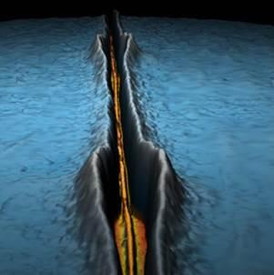 |
| Thermal gradients associated with mild heating of a metallic carbon nanotube induces thermocapillary flows in a thin organic overcoat. The result is an open trench with the tube at the base. CREDIT: J.Rogers/UIUC |
Abstract:
The exceptional properties of tiny molecular cylinders known as carbon nanotubes have tantalized researchers for years because of the possibility they could serve as a successors to silicon in laying the logic for smaller, faster and cheaper electronic devices.
Future electronics based on carbon nanotubes: A team at the University of Illinois at Urbana-Champaign finds way to purify arrays of single-walled carbon nanotubes (SWCNTs), possibly providing a step toward post-silicon circuits and devices
Washington, DC | Posted on April 7th, 2015First of all they are tiny -- on the atomic scale and perhaps near the physical limit of how small you can shrink a single electronic switch. Like silicon, they can be semiconducting in nature, a fact that is essential for circuit boards, and they can undergo fast and highly controllable electrical switching.
But a big barrier to building useful electronics with carbon nanotubes has always been the fact that when they're arrayed into films, a certain portion of them will act more like metals than semiconductors -- an unforgiving flaw that fouls the film, shorts the circuit and throws a wrench into the gears of any potential electronic device.
In fact, according to University of Illinois-Urbana Champaign professor John Rogers, the purity needs to exceed 99.999 percent -- meaning even one bad tube in 100,000 is enough to kill an electronic device. "If you have lower purity than that," he said, "that class of materials will not work for semiconducting circuits."
Now Rogers and a team of researchers have shown how to strip out the metallic carbon nanotubes from arrays using a relatively simple, scalable procedure that does not require expensive equipment. Their work is described this week in the Journal of Applied Physics, from AIP Publishing.
The Road to Purification
Though it has been a persistent problem for the last 10-15 years, the challenge of making uniform, aligned arrays of carbon nanotubes packed with good densities on thin films has largely been solved by several different groups of scientists in recent years, Rogers said.
That just left the second problem, which was to find a way to purify the material to make sure that none of the tubes were metallic in character -- a thorny problem that had remained unsolved. There were some methods of purification that were easy to do but fell far short of the level of purification necessary to make useful electronic components. Very recent approaches offer the right level of purification but rely on expensive equipment, putting the process out of reach of most researchers.
As the team reports this week, they were able to deposit a thin coating of organic material directly on top of a sheet of arrayed nanotubes in contact with a sheet of metal. They then applied current across the sheet, which allowed the current to flow through the nanotubes that were metal conductors -- but not the bulk of the tubes, which were semiconducting.
The current heated up the metal nanotubes a tiny amount -- just enough to create a "thermal capillary flow" that opened up a trench in the organic topcoat above them. Unprotected, the metallic tubes could then be etched away using a standard benchtop instrument, and then the organic topcoat could be washed away. This left an electronic wafer coated with semiconducting nanotubes free of metallic contaminants, Rogers said. They tested it by building arrays of transistors, he said.
"You end up with a device that can switch on and off as expected, based on purely semiconducting character," Rogers said.
####
About American Institute of Physics
Journal of Applied Physics is an influential international journal publishing significant new experimental and theoretical results of applied physics research. See: jap.aip.org
For more information, please click here
Contacts:
Jason Socrates Bardi
240-535-4954
Copyright © American Institute of Physics
If you have a comment, please Contact us.Issuers of news releases, not 7th Wave, Inc. or Nanotechnology Now, are solely responsible for the accuracy of the content.
Bookmark:


| Related Links |
| Related News Press |
News and information
![]() Quantum computer improves AI predictions April 17th, 2026
Quantum computer improves AI predictions April 17th, 2026
![]() Flexible sensor gains sensitivity under pressure April 17th, 2026
Flexible sensor gains sensitivity under pressure April 17th, 2026
![]() A reusable chip for particulate matter sensing April 17th, 2026
A reusable chip for particulate matter sensing April 17th, 2026
![]() Detecting vibrational quantum beating in the predissociation dynamics of SF6 using time-resolved photoelectron spectroscopy April 17th, 2026
Detecting vibrational quantum beating in the predissociation dynamics of SF6 using time-resolved photoelectron spectroscopy April 17th, 2026
Chip Technology
![]() A reusable chip for particulate matter sensing April 17th, 2026
A reusable chip for particulate matter sensing April 17th, 2026
![]() Metasurfaces smooth light to boost magnetic sensing precision January 30th, 2026
Metasurfaces smooth light to boost magnetic sensing precision January 30th, 2026
Nanotubes/Buckyballs/Fullerenes/Nanorods/Nanostrings/Nanosheets
![]() Tiny nanosheets, big leap: A new sensor detects ethanol at ultra-low levels January 30th, 2026
Tiny nanosheets, big leap: A new sensor detects ethanol at ultra-low levels January 30th, 2026
![]() Enhancing power factor of p- and n-type single-walled carbon nanotubes April 25th, 2025
Enhancing power factor of p- and n-type single-walled carbon nanotubes April 25th, 2025
![]() Chainmail-like material could be the future of armor: First 2D mechanically interlocked polymer exhibits exceptional flexibility and strength January 17th, 2025
Chainmail-like material could be the future of armor: First 2D mechanically interlocked polymer exhibits exceptional flexibility and strength January 17th, 2025
![]() Innovative biomimetic superhydrophobic coating combines repair and buffering properties for superior anti-erosion December 13th, 2024
Innovative biomimetic superhydrophobic coating combines repair and buffering properties for superior anti-erosion December 13th, 2024
Discoveries
![]() Quantum computer improves AI predictions April 17th, 2026
Quantum computer improves AI predictions April 17th, 2026
![]() Flexible sensor gains sensitivity under pressure April 17th, 2026
Flexible sensor gains sensitivity under pressure April 17th, 2026
![]() A reusable chip for particulate matter sensing April 17th, 2026
A reusable chip for particulate matter sensing April 17th, 2026
![]() Detecting vibrational quantum beating in the predissociation dynamics of SF6 using time-resolved photoelectron spectroscopy April 17th, 2026
Detecting vibrational quantum beating in the predissociation dynamics of SF6 using time-resolved photoelectron spectroscopy April 17th, 2026
Announcements
![]() A fundamentally new therapeutic approach to cystic fibrosis: Nanobody repairs cellular defect April 17th, 2026
A fundamentally new therapeutic approach to cystic fibrosis: Nanobody repairs cellular defect April 17th, 2026
![]() UC Irvine physicists discover method to reverse �quantum scrambling� : The work addresses the problem of information loss in quantum computing system April 17th, 2026
UC Irvine physicists discover method to reverse �quantum scrambling� : The work addresses the problem of information loss in quantum computing system April 17th, 2026
Interviews/Book Reviews/Essays/Reports/Podcasts/Journals/White papers/Posters
![]() A fundamentally new therapeutic approach to cystic fibrosis: Nanobody repairs cellular defect April 17th, 2026
A fundamentally new therapeutic approach to cystic fibrosis: Nanobody repairs cellular defect April 17th, 2026
![]() UC Irvine physicists discover method to reverse �quantum scrambling� : The work addresses the problem of information loss in quantum computing system April 17th, 2026
UC Irvine physicists discover method to reverse �quantum scrambling� : The work addresses the problem of information loss in quantum computing system April 17th, 2026
Research partnerships
![]() Lab to industry: InSe wafer-scale breakthrough for future electronics August 8th, 2025
Lab to industry: InSe wafer-scale breakthrough for future electronics August 8th, 2025
![]() HKU physicists uncover hidden order in the quantum world through deconfined quantum critical points April 25th, 2025
HKU physicists uncover hidden order in the quantum world through deconfined quantum critical points April 25th, 2025
|
|
||
|
|
||
| The latest news from around the world, FREE | ||
|
|
||
|
|
||
| Premium Products | ||
|
|
||
|
Only the news you want to read!
Learn More |
||
|
|
||
|
Full-service, expert consulting
Learn More |
||
|
|
||