Home > Press > Mind the gap: Nanoscale speed bump could regulate plasmons for high-speed data flow
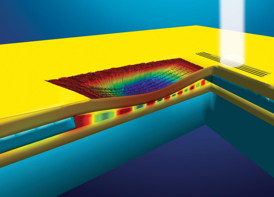 |
| The plasmonic phase modulator is an inverted, nanoscale speed bump. Gold strands are stretched side by side across a gap just 270 nanometers above the gold surface below them. Incoming plasmons travel though this air gap between the bridges and the bottom gold layer. CREDIT: Dennis/Rutgers and Dill/NIST |
Abstract:
The name sounds like something Marvin the Martian might have built, but the "nanomechanical plasmonic phase modulator" is not a doomsday device. Developed by a team of government and university researchers, including physicists from the National Institute of Standards and Technology (NIST), the innovation harnesses tiny electron waves called plasmons. It's a step towards enabling computers to process information hundreds of times faster than today's machines.
Mind the gap: Nanoscale speed bump could regulate plasmons for high-speed data flow
Gaithersburg, MD | Posted on April 1st, 2015Computers currently shuttle information around using electricity traveling down nanoscale metal wires. Although inexpensive and easy to miniaturize, metal wires are limited in terms of speed due to the resistance in the metal itself. Fiber optics use light to move information about 10,000 times faster, but these and other nonmetallic waveguides are constrained by pesky physical laws that require critical dimensions to be at least half the wavelength of the light in size; still small, but many times larger than the dimensions of current commercial nanoscale electronics.
Plasmonics combines the small size and manufacturability of electronics with the high speeds of optics. When light waves interact with electrons on a metal's surface, strong fields with dimensions far smaller than the wavelength of the original light can be created--plasmons. Unlike light, these plasmons are free to travel down nanoscale wires or gaps in metals.
The team, which included researchers from Rutgers, the University of Colorado at Colorado Springs, and Argonne National Laboratory, fabricated their device using commercial nanofabrication equipment at the NIST NanoFab. Small enough to serve in existing and future computer architectures, this technology may also enable electrically tunable and switchable thin optical components.
Their findings were published in Nature Photonics.
The plasmonic phase modulator is effectively an inverted, nanoscale speed bump. Eleven gold strands are stretched side by side like footbridges across a 23-micrometer gap just 270 nanometers above the gold surface below them. Incoming plasmons, created by laser light at one end of the array, travel though this air gap between the bridges and the bottom gold layer.
When a control voltage is applied, electrostatic attraction bends the gold strands downwards into a U shape. At a maximum voltage--close to the voltages used in today's computer chips--the gap narrows, slowing the plasmons. As the plasmons slow, their wavelength becomes shorter, allowing more than an extra half of a plasmonic wave to fit under the bridge. Because it's exactly out of phase with the original wave, this additional half wavelength can be used to selectively cancel the wave, making the bridge an optical switch.
At 23 micrometers, the prototype is relatively large, but according to NIST researcher Vladimir Aksyuk, their calculations show that the device could be shortened by a factor of 10, scaling the device's footprint down by a factor of 100. According to these calculations, the modulation range can be maintained without increase in the optical loss, as the length and the size of the gap are reduced.
"With these prototypes, we showed that nanomechanical phase tuning is efficient," says Aksyuk. "This effect can be generalized to other tunable plasmonic devices that need to be made smaller. And as they get smaller, you can put more of them on the same chip, bringing them closer to practical realization."
###
B.S. Dennis, M.I. Haftel, D.A. Czaplewski, D. Lopez, G. Blumberg and V.A. Aksyuk. Compact nano-mechanical plasmonic phase modulators. Nature Photonics. Available online March 30. 2015.
####
For more information, please click here
Contacts:
Mark Esser
301-975-8735
Copyright © National Institute of Standards and Technology (NIST)
If you have a comment, please Contact us.Issuers of news releases, not 7th Wave, Inc. or Nanotechnology Now, are solely responsible for the accuracy of the content.
Bookmark:


| Related News Press |
News and information
![]() Quantum computer improves AI predictions April 17th, 2026
Quantum computer improves AI predictions April 17th, 2026
![]() Flexible sensor gains sensitivity under pressure April 17th, 2026
Flexible sensor gains sensitivity under pressure April 17th, 2026
![]() A reusable chip for particulate matter sensing April 17th, 2026
A reusable chip for particulate matter sensing April 17th, 2026
![]() Detecting vibrational quantum beating in the predissociation dynamics of SF6 using time-resolved photoelectron spectroscopy April 17th, 2026
Detecting vibrational quantum beating in the predissociation dynamics of SF6 using time-resolved photoelectron spectroscopy April 17th, 2026
Laboratories
![]() Researchers develop molecular qubits that communicate at telecom frequencies October 3rd, 2025
Researchers develop molecular qubits that communicate at telecom frequencies October 3rd, 2025
![]() A battery�s hopping ions remember where they�ve been: Seen in atomic detail, the seemingly smooth flow of ions through a battery�s electrolyte is surprisingly complicated February 16th, 2024
A battery�s hopping ions remember where they�ve been: Seen in atomic detail, the seemingly smooth flow of ions through a battery�s electrolyte is surprisingly complicated February 16th, 2024
Govt.-Legislation/Regulation/Funding/Policy
![]() Quantum computer improves AI predictions April 17th, 2026
Quantum computer improves AI predictions April 17th, 2026
![]() Metasurfaces smooth light to boost magnetic sensing precision January 30th, 2026
Metasurfaces smooth light to boost magnetic sensing precision January 30th, 2026
![]() New imaging approach transforms study of bacterial biofilms August 8th, 2025
New imaging approach transforms study of bacterial biofilms August 8th, 2025
Chip Technology
![]() A reusable chip for particulate matter sensing April 17th, 2026
A reusable chip for particulate matter sensing April 17th, 2026
![]() Metasurfaces smooth light to boost magnetic sensing precision January 30th, 2026
Metasurfaces smooth light to boost magnetic sensing precision January 30th, 2026
Memory Technology
![]() Researchers tackle the memory bottleneck stalling quantum computing October 3rd, 2025
Researchers tackle the memory bottleneck stalling quantum computing October 3rd, 2025
![]() First real-time observation of two-dimensional melting process: Researchers at Mainz University unveil new insights into magnetic vortex structures August 8th, 2025
First real-time observation of two-dimensional melting process: Researchers at Mainz University unveil new insights into magnetic vortex structures August 8th, 2025
![]() Utilizing palladium for addressing contact issues of buried oxide thin film transistors April 5th, 2024
Utilizing palladium for addressing contact issues of buried oxide thin film transistors April 5th, 2024
Discoveries
![]() Quantum computer improves AI predictions April 17th, 2026
Quantum computer improves AI predictions April 17th, 2026
![]() Flexible sensor gains sensitivity under pressure April 17th, 2026
Flexible sensor gains sensitivity under pressure April 17th, 2026
![]() A reusable chip for particulate matter sensing April 17th, 2026
A reusable chip for particulate matter sensing April 17th, 2026
![]() Detecting vibrational quantum beating in the predissociation dynamics of SF6 using time-resolved photoelectron spectroscopy April 17th, 2026
Detecting vibrational quantum beating in the predissociation dynamics of SF6 using time-resolved photoelectron spectroscopy April 17th, 2026
Announcements
![]() A fundamentally new therapeutic approach to cystic fibrosis: Nanobody repairs cellular defect April 17th, 2026
A fundamentally new therapeutic approach to cystic fibrosis: Nanobody repairs cellular defect April 17th, 2026
![]() UC Irvine physicists discover method to reverse �quantum scrambling� : The work addresses the problem of information loss in quantum computing system April 17th, 2026
UC Irvine physicists discover method to reverse �quantum scrambling� : The work addresses the problem of information loss in quantum computing system April 17th, 2026
|
|
||
|
|
||
| The latest news from around the world, FREE | ||
|
|
||
|
|
||
| Premium Products | ||
|
|
||
|
Only the news you want to read!
Learn More |
||
|
|
||
|
Full-service, expert consulting
Learn More |
||
|
|
||