Home > Press > Chemists make new silicon-based nanomaterials
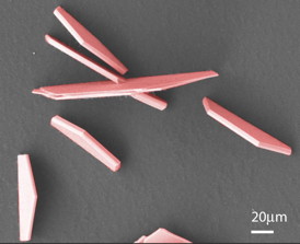 |
| Chemists from Brown University have come up with a way to make new nanomaterials from a silicon-based compound. The materials can be made in a variety of morphologies and could be used in semiconductor devices, optics or batteries. CREDIT: Koski lab / Brown University |
Abstract:
In a paper published in the journal Nanoletters, the researchers describe methods for making nanoribbons and nanoplates from a compound called silicon telluride. The materials are pure, p-type semiconductors (positive charge carriers) that could be used in a variety of electronic and optical devices. Their layered structure can take up lithium and magnesium, meaning it could also be used to make electrodes in those types of batteries.
Chemists make new silicon-based nanomaterials
Providence, RI | Posted on March 27th, 2015"Silicon-based compounds are the backbone of modern electronics processing," said Kristie Koski, assistant professor of chemistry at Brown, who led the work. "Silicon telluride is in that family of compounds, and we've shown a totally new method for using it to make layered, two-dimensional nanomaterials."
Koski and her team synthesized the new materials through vapor deposition in a tube furnace. When heated in the tube, silicon and tellurium vaporize and react to make a precursor compound that is deposited on a substrate by an argon carrier gas. The silicon telluride then grows from the precursor compound.
Different structures can be made by varying the furnace temperature and using different treatments of the substrate. By tweaking the process, the researchers made nanoribbons that are about 50 to 1,000 nanometers in width and about 10 microns long. They also made nanoplates flat on the substrate and standing upright.
"We see the standing plates a lot," Koski said. "They're half hexagons sitting upright on the substrate. They look a little like a graveyard."
Each of the different shapes has a different orientation of the material's crystalline structure. As a result, they all have different properties and could be used in different applications.
The researchers also showed that the material can be "doped" through the use of different substrates. Doping is a process through which tiny impurities are introduced to change a material's electrical prosperities. In this case, the researchers showed that silicon telluride can be doped with aluminum when grown on a sapphire substrate. That process could be used, for example, to change the material from a p-type semiconductor (one with positive charge carriers) to an n-type (one with negative charge carriers).
The materials are not particularly stable out in the environment, Koski says, but that's easily remedied.
"What we can do is oxidize the silicon telluride and then bake off the tellurium, leaving a coating of silicon oxide," she said. "That coating protects it and it stays pretty stable."
From here, Koski and her team plan to continue testing the material's electronic and optical properties. They're encouraged by what they've seen so far.
"We think this is a good candidate for bringing the properties of 2-D materials into the realm of electronics," Koski said.
####
For more information, please click here
Contacts:
Kevin Stacey
401-863-3766
Copyright © Brown University
If you have a comment, please Contact us.Issuers of news releases, not 7th Wave, Inc. or Nanotechnology Now, are solely responsible for the accuracy of the content.
Bookmark:


| Related Links |
![]() The paper is available at the following link:
The paper is available at the following link:
| Related News Press |
News and information
![]() Quantum computer improves AI predictions April 17th, 2026
Quantum computer improves AI predictions April 17th, 2026
![]() Flexible sensor gains sensitivity under pressure April 17th, 2026
Flexible sensor gains sensitivity under pressure April 17th, 2026
![]() A reusable chip for particulate matter sensing April 17th, 2026
A reusable chip for particulate matter sensing April 17th, 2026
![]() Detecting vibrational quantum beating in the predissociation dynamics of SF6 using time-resolved photoelectron spectroscopy April 17th, 2026
Detecting vibrational quantum beating in the predissociation dynamics of SF6 using time-resolved photoelectron spectroscopy April 17th, 2026
Chemistry
![]() Projecting light to dispense liquids: A new route to ultra-precise microdroplets January 30th, 2026
Projecting light to dispense liquids: A new route to ultra-precise microdroplets January 30th, 2026
![]() From sensors to smart systems: the rise of AI-driven photonic noses January 30th, 2026
From sensors to smart systems: the rise of AI-driven photonic noses January 30th, 2026
![]() "Nanoreactor" cage uses visible light for catalytic and ultra-selective cross-cycloadditions October 3rd, 2025
"Nanoreactor" cage uses visible light for catalytic and ultra-selective cross-cycloadditions October 3rd, 2025
![]() Cambridge chemists discover simple way to build bigger molecules � one carbon at a time June 6th, 2025
Cambridge chemists discover simple way to build bigger molecules � one carbon at a time June 6th, 2025
Discoveries
![]() Quantum computer improves AI predictions April 17th, 2026
Quantum computer improves AI predictions April 17th, 2026
![]() Flexible sensor gains sensitivity under pressure April 17th, 2026
Flexible sensor gains sensitivity under pressure April 17th, 2026
![]() A reusable chip for particulate matter sensing April 17th, 2026
A reusable chip for particulate matter sensing April 17th, 2026
![]() Detecting vibrational quantum beating in the predissociation dynamics of SF6 using time-resolved photoelectron spectroscopy April 17th, 2026
Detecting vibrational quantum beating in the predissociation dynamics of SF6 using time-resolved photoelectron spectroscopy April 17th, 2026
Materials/Metamaterials/Magnetoresistance
![]() First real-time observation of two-dimensional melting process: Researchers at Mainz University unveil new insights into magnetic vortex structures August 8th, 2025
First real-time observation of two-dimensional melting process: Researchers at Mainz University unveil new insights into magnetic vortex structures August 8th, 2025
![]() Researchers unveil a groundbreaking clay-based solution to capture carbon dioxide and combat climate change June 6th, 2025
Researchers unveil a groundbreaking clay-based solution to capture carbon dioxide and combat climate change June 6th, 2025
![]() A 1960s idea inspires NBI researchers to study hitherto inaccessible quantum states June 6th, 2025
A 1960s idea inspires NBI researchers to study hitherto inaccessible quantum states June 6th, 2025
![]() Institute for Nanoscience hosts annual proposal planning meeting May 16th, 2025
Institute for Nanoscience hosts annual proposal planning meeting May 16th, 2025
Announcements
![]() A fundamentally new therapeutic approach to cystic fibrosis: Nanobody repairs cellular defect April 17th, 2026
A fundamentally new therapeutic approach to cystic fibrosis: Nanobody repairs cellular defect April 17th, 2026
![]() UC Irvine physicists discover method to reverse �quantum scrambling� : The work addresses the problem of information loss in quantum computing system April 17th, 2026
UC Irvine physicists discover method to reverse �quantum scrambling� : The work addresses the problem of information loss in quantum computing system April 17th, 2026
Interviews/Book Reviews/Essays/Reports/Podcasts/Journals/White papers/Posters
![]() A fundamentally new therapeutic approach to cystic fibrosis: Nanobody repairs cellular defect April 17th, 2026
A fundamentally new therapeutic approach to cystic fibrosis: Nanobody repairs cellular defect April 17th, 2026
![]() UC Irvine physicists discover method to reverse �quantum scrambling� : The work addresses the problem of information loss in quantum computing system April 17th, 2026
UC Irvine physicists discover method to reverse �quantum scrambling� : The work addresses the problem of information loss in quantum computing system April 17th, 2026
Battery Technology/Capacitors/Generators/Piezoelectrics/Thermoelectrics/Energy storage
![]() Decoding hydrogen‑bond network of electrolyte for cryogenic durable aqueous zinc‑ion batteries January 30th, 2026
Decoding hydrogen‑bond network of electrolyte for cryogenic durable aqueous zinc‑ion batteries January 30th, 2026
![]() COF scaffold membrane with gate‑lane nanostructure for efficient Li+/Mg2+ separation January 30th, 2026
COF scaffold membrane with gate‑lane nanostructure for efficient Li+/Mg2+ separation January 30th, 2026
![]() MXene nanomaterials enter a new dimension Multilayer nanomaterial: MXene flakes created at Drexel University show new promise as 1D scrolls January 30th, 2026
MXene nanomaterials enter a new dimension Multilayer nanomaterial: MXene flakes created at Drexel University show new promise as 1D scrolls January 30th, 2026
Photonics/Optics/Lasers
![]() Metasurfaces smooth light to boost magnetic sensing precision January 30th, 2026
Metasurfaces smooth light to boost magnetic sensing precision January 30th, 2026
![]() From sensors to smart systems: the rise of AI-driven photonic noses January 30th, 2026
From sensors to smart systems: the rise of AI-driven photonic noses January 30th, 2026
|
|
||
|
|
||
| The latest news from around the world, FREE | ||
|
|
||
|
|
||
| Premium Products | ||
|
|
||
|
Only the news you want to read!
Learn More |
||
|
|
||
|
Full-service, expert consulting
Learn More |
||
|
|
||