Home > Press > A graphene solution for microwave interference
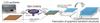 |
| "Graphene-PMMA heterostructure (from Batrakov et al., Nature Sci. Rep. 4:7191 (2014) - Creative Commons licence CC BY-NC-ND 4.0)" |
Abstract:
Microwave communication is ubiquitous in the modern world, with electromagnetic waves in the tens of gigahertz range providing efficient transmission with wide bandwidth for data links between Earth-orbiting satellites and ground stations. Such ultra-high frequency wireless communication is now so common, with a resultant crowding of the spectral bands allocated to different communications channels, that interference and electromagnetic compatibility (EMC) are serious concerns.
A graphene solution for microwave interference
Cambridge, UK | Posted on March 23rd, 2015Rules governing EMC dictate that new equipment meet stringent requirements concerning microwave shielding of both components and systems. This is driving a search for new materials to be used as coating layers, shields and filters in future nanoelectronic devices.
Shielding electronic devices with a barrier that simply reflects incoming microwave radiation only shifts the electromagnetic pollution problem elsewhere. The research focus is therefore on developing EMC coatings that absorb rather than reflect microwaves, with a practical emphasis on layers less than a thousandth of a millimetre thick.
A team of physicists led by Philippe Lambin from the Universit� de Namur in Belgium has found that a graphene plane can provide an effective absorbent shield against microwaves. The results of the study, the principal contributors to which are Konstantin Batrakov and Polina Kuzhir, both from the Belarussian State University in Minsk, are published in the journal Nature Scientific Reports. All eight of the authors are part of the Graphene Flagship, a consortium of academic and industrial partners that focuses on the need for Europe to address the big scientific and technological challenges through long-term, multidisciplinary research efforts.
Lambin and his colleagues demonstrated that the conductivity of several graphene layers adds arithmetically when thin polymer spacers separate them. Maximum microwave absorption in the Ka communications band between 26.5 and 40 GHz is achieved with six graphene planes separated by layers of poly-methyl methacrylate (PMMA), a transparent plastic also known as acrylic glass.
Multilayer microwave barriers constructed by researchers based at Joensuu University in Finland start with a first graphene layer deposited on a copper foil substrate by chemical vapour deposition. This layer is then covered with a 600-800 nanometre PMMA spacer obtained by spin coating, following which the copper is etched away with ferric chloride, and the graphene/PMMA heterostructure transferred to a quartz substrate. The procedure is repeated until the required number of graphene layers is reached.
A single layer of graphene can absorb up to 25% of incident microwave radiation, which is a lot for a one atom-thick material. With a multilayer graphene/PMMA arrangement, the absorption rises to 50%. This can be understood by analysing the transmission and reflection of a plane wave at the interface between two dielectric media, when the interface contains an infinitesimally thin conducting layer. In this way, the researchers were able to optimise their graphene-PMMA structures for maximum absorption, with the results confirmed by rigorous electromagnetic testing.
Moreover, notes Lambin, there is the interface between the shielding material and air to consider...
"We have found that the static conductivity of graphene is close to the value which relates the magnetic and electric fields in any electromagnetic radiation propagating in air. Thanks to this happy coincidence, graphene is an ideal material for absorbing radio waves, thus protecting sensitive electronic devices."
The idea of using graphene/dielectric multilayers for electromagnetic wave absorption is not new. For example, a few years ago there was published a theoretical proposal for an ultra-broadband absorbing multilayer operating in the terahertz region, far higher than the Ka communications band discussed here.
A multilayer terahertz shield would be a complex affair, with its graphene planes patterned at the micron scale in order to generate surface plasmon resonances - oscillations in the electrons which propagate along the interfaces between different material layers. The microwave barrier devised by the Graphene Flagship team is relatively simple by comparison, with advantages in terms of fabrication and scalability.
In real-world applications, graphene/PMMA multilayers require protection against external chemical and mechanical agents. The quartz substrate should therefore face outwards, and be combined with a softer material. The choice and thickness of over-layer material used are additional parameters that will influence the microwave absorbance.
Process scalability will increase considerably if stacks of few-layer graphene are deposited in one step, instead of piling up graphene monolayers with their PMMA shuttles. In addition, any process that raises the conductivity of graphene will reduce the number of atomic planes required to maximise the level of microwave absorption.
Francis Sedgemore, Science Writer, Graphene Flagship
####
About Graphene Flagship
The Graphene Flagship is the EU�s biggest research initiative ever, and, according to the European Commission, �history�s greatest distinction for excellent research�. With a budget of EUR one billion, the Graphene Flagship is tasked with taking graphene from the realm of academic laboratories into European society in the space of ten years, thus generating economic growth, new jobs and new opportunities for Europeans as both investors and employees.
For more information, please click here
Contacts:
Francis Sedgemore
Graphene Flagship
+44 1223 748344
Copyright © AlphaGalileo
If you have a comment, please Contact us.Issuers of news releases, not 7th Wave, Inc. or Nanotechnology Now, are solely responsible for the accuracy of the content.
Bookmark:


| Related Links |
| Related News Press |
News and information
![]() Quantum computer improves AI predictions April 17th, 2026
Quantum computer improves AI predictions April 17th, 2026
![]() Flexible sensor gains sensitivity under pressure April 17th, 2026
Flexible sensor gains sensitivity under pressure April 17th, 2026
![]() A reusable chip for particulate matter sensing April 17th, 2026
A reusable chip for particulate matter sensing April 17th, 2026
![]() Detecting vibrational quantum beating in the predissociation dynamics of SF6 using time-resolved photoelectron spectroscopy April 17th, 2026
Detecting vibrational quantum beating in the predissociation dynamics of SF6 using time-resolved photoelectron spectroscopy April 17th, 2026
Wireless/telecommunications/RF/Antennas/Microwaves
![]() Researchers develop molecular qubits that communicate at telecom frequencies October 3rd, 2025
Researchers develop molecular qubits that communicate at telecom frequencies October 3rd, 2025
Graphene/ Graphite
![]() Electrifying results shed light on graphene foam as a potential material for lab grown cartilage June 6th, 2025
Electrifying results shed light on graphene foam as a potential material for lab grown cartilage June 6th, 2025
![]() Breakthrough in proton barrier films using pore-free graphene oxide: Kumamoto University researchers achieve new milestone in advanced coating technologies September 13th, 2024
Breakthrough in proton barrier films using pore-free graphene oxide: Kumamoto University researchers achieve new milestone in advanced coating technologies September 13th, 2024
Discoveries
![]() Quantum computer improves AI predictions April 17th, 2026
Quantum computer improves AI predictions April 17th, 2026
![]() Flexible sensor gains sensitivity under pressure April 17th, 2026
Flexible sensor gains sensitivity under pressure April 17th, 2026
![]() A reusable chip for particulate matter sensing April 17th, 2026
A reusable chip for particulate matter sensing April 17th, 2026
![]() Detecting vibrational quantum beating in the predissociation dynamics of SF6 using time-resolved photoelectron spectroscopy April 17th, 2026
Detecting vibrational quantum beating in the predissociation dynamics of SF6 using time-resolved photoelectron spectroscopy April 17th, 2026
Announcements
![]() A fundamentally new therapeutic approach to cystic fibrosis: Nanobody repairs cellular defect April 17th, 2026
A fundamentally new therapeutic approach to cystic fibrosis: Nanobody repairs cellular defect April 17th, 2026
![]() UC Irvine physicists discover method to reverse �quantum scrambling� : The work addresses the problem of information loss in quantum computing system April 17th, 2026
UC Irvine physicists discover method to reverse �quantum scrambling� : The work addresses the problem of information loss in quantum computing system April 17th, 2026
Interviews/Book Reviews/Essays/Reports/Podcasts/Journals/White papers/Posters
![]() A fundamentally new therapeutic approach to cystic fibrosis: Nanobody repairs cellular defect April 17th, 2026
A fundamentally new therapeutic approach to cystic fibrosis: Nanobody repairs cellular defect April 17th, 2026
![]() UC Irvine physicists discover method to reverse �quantum scrambling� : The work addresses the problem of information loss in quantum computing system April 17th, 2026
UC Irvine physicists discover method to reverse �quantum scrambling� : The work addresses the problem of information loss in quantum computing system April 17th, 2026
|
|
||
|
|
||
| The latest news from around the world, FREE | ||
|
|
||
|
|
||
| Premium Products | ||
|
|
||
|
Only the news you want to read!
Learn More |
||
|
|
||
|
Full-service, expert consulting
Learn More |
||
|
|
||