Home > Press > Imec Demonstrates Compact Wavelength-Division Multiplexing CMOS Silicon Photonics Transceiver
 |
Abstract:
Today, at the 2015 International Solid State Circuits Conference (ISSCC), nanoelectronics research center imec, in collaboration with Tyndall National Institute, the University of Leuven (KULeuven) and the Ghent University, demonstrated a 4x20Gb/s wavelength division multiplexing (WDM) hybrid CMOS silicon photonics transceiver, paving the way to cost-effective, high-density single-mode optical fiber links.
Imec Demonstrates Compact Wavelength-Division Multiplexing CMOS Silicon Photonics Transceiver
San Francisco, CA | Posted on March 1st, 2015Hybrid CMOS silicon photonics transceivers, transmitting and receiving data over single-mode optical fiber, are expected to play a key role in next-generation datacenter connectivity. By leveraging existing CMOS manufacturing and 3-D assembly infrastructure, the hybrid CMOS silicon photonics platform enables high integration density and reduced power consumption, as well as high yield and low manufacturing cost. Combined with wavelength division multiplexing capability, highly scalable single-mode optical transceivers can be constructed, satisfying the growing need for interconnect bandwidth in next-generation cloud infrastructure.
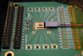
Imec's CMOS silicon photonics transceiver comprises a silicon photonics (SiPh) chip, flip-chip integrated with a low-power 40nm CMOS chip. The SiPh chip, fabricated on imec's 25Gb/s Silicon Photonics Platform (iSiPP25G), comprises an array of four compact 25Gb/s ring modulators, coupled to a common bus waveguide to allow WDM transmission. On the receive side, a ring-based, low-loss (2dB) demultiplexing filter with 300GHz channel spacing is implemented and further connected to an array of four 25Gb/s Ge waveguide photodetectors. Both the ring modulators and the ring WDM filters include highly efficient integrated heating elements to tune their resonant wavelengths to the desired WDM channels. The CMOS chip includes four differential 20Gb/s ring modulator drivers and four 20Gb/s trans-impedance amplifiers. A 12 channel single-mode fiber array is packaged onto the grating coupler array on the chip, using a planar approach developed at Tyndall National Institute.
Error-free operation was demonstrated in a 20Gb/s loop-back experiment for all four WDM channels as well as with two channels running together. The dynamic power consumption of the transceiver, including the CMOS driver and receiver, was less than 2pJ/bit. Thermal tuning of the WDM channel wavelengths consumed only 7mW/nm per channel. The transceiver can be further scaled to higher bandwidth capacity by adopting more advanced CMOS technology and by adding more WDM channels, enabling optical modules for 100GbE, 400GbE and beyond for future datacenter interconnects.
This work was supported by imec's optical I/O core partner program. Imec's iSiPP25G technology can be accessed through Europractice, while Si Photonics packaging services are available through Tyndall National Institute (Ireland).
####
About IMEC
Imec performs world-leading research in nanoelectronics and photovoltaics. Imec leverages its scientific knowledge with the innovative power of its global partnerships in ICT, healthcare and energy. Imec delivers industry-relevant technology solutions. In a unique high-tech environment, its international top talent is committed to providing the building blocks for a better life in a sustainable society. Imec is headquartered in Leuven, Belgium, and has offices in the Netherlands, Taiwan, U.S., China, India and Japan. Its staff of over 2,080 people includes more than 670 industrial residents and guest researchers. In 2013, imec's revenue (P&L) totaled 332 million euro. Further information on imec can be found at www.imec.be. Stay up to date about what�s happening at imec with the monthly imec magazine, available for tablets and smartphones (as an app for�iOS�and�Android), or via the website www.imec.be/imecmagazine
Imec is a registered trademark for the activities of IMEC International (a legal entity set up under Belgian law as a "stichting van openbaar nut�), imec Belgium (IMEC vzw supported by the Flemish Government), imec the Netherlands (Stichting IMEC Nederland, part of Holst Centre which is supported by the Dutch Government), imec Taiwan (IMEC Taiwan Co.)and imec China (IMEC Microelectronics (Shanghai) Co. Ltd.) and imec India (Imec India Private Limited).
About Europractice
The EUROPRACTICE IC Service brings ASIC design and manufacturing capability within the technical and financial reach of any company that wishes to use ASICs.
The EUROPRACTICE IC Service, offered by IMEC and Fraunhofer, offers low-cost ASIC prototyping and ASIC small volume production ramp-up to high volume production through Multi Project Wafer - MPW - and dedicated wafer runs.
More information: www.europractice-ic.com/
For more information, please click here
Contacts:
Stephanie Black
Business Technology
[f o r m u l a]
Havas Formula
Office 619-234-0345
Copyright © IMEC
If you have a comment, please Contact us.Issuers of news releases, not 7th Wave, Inc. or Nanotechnology Now, are solely responsible for the accuracy of the content.
Bookmark:


| Related News Press |
News and information
![]() Quantum computer improves AI predictions April 17th, 2026
Quantum computer improves AI predictions April 17th, 2026
![]() Flexible sensor gains sensitivity under pressure April 17th, 2026
Flexible sensor gains sensitivity under pressure April 17th, 2026
![]() A reusable chip for particulate matter sensing April 17th, 2026
A reusable chip for particulate matter sensing April 17th, 2026
![]() Detecting vibrational quantum beating in the predissociation dynamics of SF6 using time-resolved photoelectron spectroscopy April 17th, 2026
Detecting vibrational quantum beating in the predissociation dynamics of SF6 using time-resolved photoelectron spectroscopy April 17th, 2026
Wireless/telecommunications/RF/Antennas/Microwaves
![]() Researchers develop molecular qubits that communicate at telecom frequencies October 3rd, 2025
Researchers develop molecular qubits that communicate at telecom frequencies October 3rd, 2025
![]() HKUST researchers develop new integration technique for efficient coupling of III-V and silicon February 16th, 2024
HKUST researchers develop new integration technique for efficient coupling of III-V and silicon February 16th, 2024
Discoveries
![]() Quantum computer improves AI predictions April 17th, 2026
Quantum computer improves AI predictions April 17th, 2026
![]() Flexible sensor gains sensitivity under pressure April 17th, 2026
Flexible sensor gains sensitivity under pressure April 17th, 2026
![]() A reusable chip for particulate matter sensing April 17th, 2026
A reusable chip for particulate matter sensing April 17th, 2026
![]() Detecting vibrational quantum beating in the predissociation dynamics of SF6 using time-resolved photoelectron spectroscopy April 17th, 2026
Detecting vibrational quantum beating in the predissociation dynamics of SF6 using time-resolved photoelectron spectroscopy April 17th, 2026
Announcements
![]() A fundamentally new therapeutic approach to cystic fibrosis: Nanobody repairs cellular defect April 17th, 2026
A fundamentally new therapeutic approach to cystic fibrosis: Nanobody repairs cellular defect April 17th, 2026
![]() UC Irvine physicists discover method to reverse �quantum scrambling� : The work addresses the problem of information loss in quantum computing system April 17th, 2026
UC Irvine physicists discover method to reverse �quantum scrambling� : The work addresses the problem of information loss in quantum computing system April 17th, 2026
Events/Classes
![]() Institute for Nanoscience hosts annual proposal planning meeting May 16th, 2025
Institute for Nanoscience hosts annual proposal planning meeting May 16th, 2025
![]() A New Blue: Mysterious origin of the ribbontail ray�s electric blue spots revealed July 5th, 2024
A New Blue: Mysterious origin of the ribbontail ray�s electric blue spots revealed July 5th, 2024
![]() Researchers demonstrate co-propagation of quantum and classical signals: Study shows that quantum encryption can be implemented in existing fiber networks January 20th, 2023
Researchers demonstrate co-propagation of quantum and classical signals: Study shows that quantum encryption can be implemented in existing fiber networks January 20th, 2023
Photonics/Optics/Lasers
![]() Metasurfaces smooth light to boost magnetic sensing precision January 30th, 2026
Metasurfaces smooth light to boost magnetic sensing precision January 30th, 2026
![]() From sensors to smart systems: the rise of AI-driven photonic noses January 30th, 2026
From sensors to smart systems: the rise of AI-driven photonic noses January 30th, 2026
Alliances/Trade associations/Partnerships/Distributorships
![]() Chicago Quantum Exchange welcomes six new partners highlighting quantum technology solutions, from Chicago and beyond September 23rd, 2022
Chicago Quantum Exchange welcomes six new partners highlighting quantum technology solutions, from Chicago and beyond September 23rd, 2022
![]() University of Illinois Chicago joins Brookhaven Lab's Quantum Center June 10th, 2022
University of Illinois Chicago joins Brookhaven Lab's Quantum Center June 10th, 2022
Research partnerships
![]() Lab to industry: InSe wafer-scale breakthrough for future electronics August 8th, 2025
Lab to industry: InSe wafer-scale breakthrough for future electronics August 8th, 2025
![]() HKU physicists uncover hidden order in the quantum world through deconfined quantum critical points April 25th, 2025
HKU physicists uncover hidden order in the quantum world through deconfined quantum critical points April 25th, 2025
|
|
||
|
|
||
| The latest news from around the world, FREE | ||
|
|
||
|
|
||
| Premium Products | ||
|
|
||
|
Only the news you want to read!
Learn More |
||
|
|
||
|
Full-service, expert consulting
Learn More |
||
|
|
||