Home > Press > Penn researchers develop new technique for making molybdenum disulfide: Extra control over monolayer material with advantages over graphene
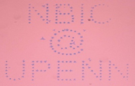 |
| "Seeding" the growth of molybdenum disulphide flakes gave the researches enough control over their location to spell a message. |
Abstract:
Graphene, a single-atom-thick lattice of carbon atoms, is often touted as a replacement for silicon in electronic devices due to its extremely high conductivity and unbeatable thinness. But graphene is not the only two-dimensional material that could play such a role.
Penn researchers develop new technique for making molybdenum disulfide: Extra control over monolayer material with advantages over graphene
Philadelphia, PA | Posted on February 19th, 2015University of Pennsylvania researchers have made an advance in manufacturing one such material, molybdenum disulphide. By growing flakes of the material around "seeds" of molybdenum oxide, they have made it easier to control the size, thickness and location of the material.
Unlike graphene, molybdenum disulfide has an energy band gap, meaning its conductivity can be turned on and off. Such a trait is critical for semiconductor devices used in computing. Another difference is that molybdenum disulphide emits light, meaning it could be used in applications like LEDs, self-reporting sensors and optoelectronics.
The study was led by A. T. Charlie Johnson, professor in the Department of Physics & Astronomy in Penn's School of Arts & Sciences, and includes members of his lab, Gang Hee Han, Nicholas Kybert, Carl Naylor and Jinglei Ping. Also contributing to the study was Ritesh Agarwal, professor of materials science and engineering in Penn's School of Engineering and Applied Science; members of his lab, Bumsu Lee and Joohee Park; and Jisoo Kang, a master's student in Penn's nanotechnology program. They collaborated with researchers from South Korea's Sungkyunkwan University, Si Young Lee and Young Hee Lee.
Their study was published in the journal Nature Communications.
"Everything we do with regular electronics we'd like to be able to do with two-dimensional materials," Johnson said. "Graphene has one set of properties that make it very attractive for electronics, but it lacks this critical property, being able to turn on and off. Molybdenum disulphide gives you that."
Graphene's ultra-high conductivity means that it can move electrons more quickly than any known material, but that is not the only quality that matters for electronics. For the transistors that form the basis for modern computing technology, being able to stop the flow of electrons is also critical.
"Molybdenum disulphide is not as conductive as graphene," Naylor said, "but it has a very high on/off ratio. We need 1's and 0's to do computation; graphene can only give us 1's and .5's."
Other research groups have been able to make small flakes of molybdenum disulphide the same way graphene was first made, by exfoliating it, or peeling off atomically thin layers from the bulk material. More recently, other researchers have adopted another technique from graphene manufacture, chemical vapor deposition, where the molybdenum and sulfur are heated into gasses and left to settle and crystalize on a substrate.
The problem with these methods is that the resulting flakes form in a scattershot way.
"Between hunting down the flakes," said Kybert, "and making sure they're the right size and thickness, it would take days to make a single measurement of their properties"
The Penn team's advance was in developing a way to control where the flakes form in the chemical vapor deposition method, by "seeding" the substrate with a precursor.
"We start by placing down a small amount of molybdenum oxide in the locations we want," Naylor said, "then we flow in sulfur gas. Under the right conditions, those seeds react with sulfur and flakes of molybdenum disulphide being to grow."
"There's finesse involved in optimizing the growth conditions," Johnson said, "but we're exerting more control, moving the material in the direction of being able to make complicated systems. Because we grow it where we want it, we can make devices more easily. We have all of the other parts of the transistors in a separate layer that we snap down on top of the flakes, making dozens and potentially even hundreds, of devices at once. Then we were able to observe that we made transistors that turned on and off like they were supposed to and devices that emit light like they are supposed to."
Being able to match up the location of the molybdenum disulphide flakes with corresponding electronics allowed the researchers to skip a step they must take when making graphene-based devices. There, graphene is grown in large sheets and then cut down to size, a process that adds to the risk of damaging contamination.
Future work on these molybdenum disulphide devices will complement the research team's research on graphene-based biosensors; rather than outputting the detection of some molecule to a computer, molybdenum disulfide-based sensors could directly report a binding event through a change in the light they emit.
This research also represents first steps that can be applied toward fabricating a new family of two-dimensional materials.
"We can replace the molybdenum with tungsten and the sulfur with selenium," Naylor said, "and just go down the periodic table from there. We can imagine growing all of these different materials in the places we choose and taking advantages of all of their different properties."
###
The research was supported by the National Science Foundation through its Accelerating Innovation in Research Program AIR ENG-1312202, the Nano/Bio Interface Center through NSF's Nanoscale Science and Engineering Center program DMR08-32802, the Laboratory for Research on the Structure of Matter through the NSF's Materials Research Science and Engineering Center program DMR-1120901, the National Institutes of Health though the NIH Director's New Innovator Award Program 1-DP2-7251-01 and the U.S. Army Research Office under grant W911NF-11-1-0024.
####
For more information, please click here
Contacts:
Evan Lerner
215-573-6604
Copyright © University of Pennsylvania
If you have a comment, please Contact us.Issuers of news releases, not 7th Wave, Inc. or Nanotechnology Now, are solely responsible for the accuracy of the content.
Bookmark:


| Related News Press |
News and information
![]() Quantum computer improves AI predictions April 17th, 2026
Quantum computer improves AI predictions April 17th, 2026
![]() Flexible sensor gains sensitivity under pressure April 17th, 2026
Flexible sensor gains sensitivity under pressure April 17th, 2026
![]() A reusable chip for particulate matter sensing April 17th, 2026
A reusable chip for particulate matter sensing April 17th, 2026
![]() Detecting vibrational quantum beating in the predissociation dynamics of SF6 using time-resolved photoelectron spectroscopy April 17th, 2026
Detecting vibrational quantum beating in the predissociation dynamics of SF6 using time-resolved photoelectron spectroscopy April 17th, 2026
Display technology/LEDs/SS Lighting/OLEDs
![]() Spinel-type sulfide semiconductors to operate the next-generation LEDs and solar cells For solar-cell absorbers and green-LED source October 3rd, 2025
Spinel-type sulfide semiconductors to operate the next-generation LEDs and solar cells For solar-cell absorbers and green-LED source October 3rd, 2025
Graphene/ Graphite
![]() Electrifying results shed light on graphene foam as a potential material for lab grown cartilage June 6th, 2025
Electrifying results shed light on graphene foam as a potential material for lab grown cartilage June 6th, 2025
![]() Breakthrough in proton barrier films using pore-free graphene oxide: Kumamoto University researchers achieve new milestone in advanced coating technologies September 13th, 2024
Breakthrough in proton barrier films using pore-free graphene oxide: Kumamoto University researchers achieve new milestone in advanced coating technologies September 13th, 2024
Govt.-Legislation/Regulation/Funding/Policy
![]() Quantum computer improves AI predictions April 17th, 2026
Quantum computer improves AI predictions April 17th, 2026
![]() Metasurfaces smooth light to boost magnetic sensing precision January 30th, 2026
Metasurfaces smooth light to boost magnetic sensing precision January 30th, 2026
![]() New imaging approach transforms study of bacterial biofilms August 8th, 2025
New imaging approach transforms study of bacterial biofilms August 8th, 2025
Chip Technology
![]() A reusable chip for particulate matter sensing April 17th, 2026
A reusable chip for particulate matter sensing April 17th, 2026
![]() Metasurfaces smooth light to boost magnetic sensing precision January 30th, 2026
Metasurfaces smooth light to boost magnetic sensing precision January 30th, 2026
Sensors
![]() Flexible sensor gains sensitivity under pressure April 17th, 2026
Flexible sensor gains sensitivity under pressure April 17th, 2026
![]() Tiny nanosheets, big leap: A new sensor detects ethanol at ultra-low levels January 30th, 2026
Tiny nanosheets, big leap: A new sensor detects ethanol at ultra-low levels January 30th, 2026
![]() From sensors to smart systems: the rise of AI-driven photonic noses January 30th, 2026
From sensors to smart systems: the rise of AI-driven photonic noses January 30th, 2026
![]() Sensors innovations for smart lithium-based batteries: advancements, opportunities, and potential challenges August 8th, 2025
Sensors innovations for smart lithium-based batteries: advancements, opportunities, and potential challenges August 8th, 2025
Discoveries
![]() Quantum computer improves AI predictions April 17th, 2026
Quantum computer improves AI predictions April 17th, 2026
![]() Flexible sensor gains sensitivity under pressure April 17th, 2026
Flexible sensor gains sensitivity under pressure April 17th, 2026
![]() A reusable chip for particulate matter sensing April 17th, 2026
A reusable chip for particulate matter sensing April 17th, 2026
![]() Detecting vibrational quantum beating in the predissociation dynamics of SF6 using time-resolved photoelectron spectroscopy April 17th, 2026
Detecting vibrational quantum beating in the predissociation dynamics of SF6 using time-resolved photoelectron spectroscopy April 17th, 2026
Materials/Metamaterials/Magnetoresistance
![]() First real-time observation of two-dimensional melting process: Researchers at Mainz University unveil new insights into magnetic vortex structures August 8th, 2025
First real-time observation of two-dimensional melting process: Researchers at Mainz University unveil new insights into magnetic vortex structures August 8th, 2025
![]() Researchers unveil a groundbreaking clay-based solution to capture carbon dioxide and combat climate change June 6th, 2025
Researchers unveil a groundbreaking clay-based solution to capture carbon dioxide and combat climate change June 6th, 2025
![]() A 1960s idea inspires NBI researchers to study hitherto inaccessible quantum states June 6th, 2025
A 1960s idea inspires NBI researchers to study hitherto inaccessible quantum states June 6th, 2025
![]() Institute for Nanoscience hosts annual proposal planning meeting May 16th, 2025
Institute for Nanoscience hosts annual proposal planning meeting May 16th, 2025
Announcements
![]() A fundamentally new therapeutic approach to cystic fibrosis: Nanobody repairs cellular defect April 17th, 2026
A fundamentally new therapeutic approach to cystic fibrosis: Nanobody repairs cellular defect April 17th, 2026
![]() UC Irvine physicists discover method to reverse �quantum scrambling� : The work addresses the problem of information loss in quantum computing system April 17th, 2026
UC Irvine physicists discover method to reverse �quantum scrambling� : The work addresses the problem of information loss in quantum computing system April 17th, 2026
Interviews/Book Reviews/Essays/Reports/Podcasts/Journals/White papers/Posters
![]() A fundamentally new therapeutic approach to cystic fibrosis: Nanobody repairs cellular defect April 17th, 2026
A fundamentally new therapeutic approach to cystic fibrosis: Nanobody repairs cellular defect April 17th, 2026
![]() UC Irvine physicists discover method to reverse �quantum scrambling� : The work addresses the problem of information loss in quantum computing system April 17th, 2026
UC Irvine physicists discover method to reverse �quantum scrambling� : The work addresses the problem of information loss in quantum computing system April 17th, 2026
Military
![]() Quantum engineers �squeeze� laser frequency combs to make more sensitive gas sensors January 17th, 2025
Quantum engineers �squeeze� laser frequency combs to make more sensitive gas sensors January 17th, 2025
![]() Chainmail-like material could be the future of armor: First 2D mechanically interlocked polymer exhibits exceptional flexibility and strength January 17th, 2025
Chainmail-like material could be the future of armor: First 2D mechanically interlocked polymer exhibits exceptional flexibility and strength January 17th, 2025
![]() Single atoms show their true color July 5th, 2024
Single atoms show their true color July 5th, 2024
![]() NRL charters Navy�s quantum inertial navigation path to reduce drift April 5th, 2024
NRL charters Navy�s quantum inertial navigation path to reduce drift April 5th, 2024
Research partnerships
![]() Lab to industry: InSe wafer-scale breakthrough for future electronics August 8th, 2025
Lab to industry: InSe wafer-scale breakthrough for future electronics August 8th, 2025
![]() HKU physicists uncover hidden order in the quantum world through deconfined quantum critical points April 25th, 2025
HKU physicists uncover hidden order in the quantum world through deconfined quantum critical points April 25th, 2025
|
|
||
|
|
||
| The latest news from around the world, FREE | ||
|
|
||
|
|
||
| Premium Products | ||
|
|
||
|
Only the news you want to read!
Learn More |
||
|
|
||
|
Full-service, expert consulting
Learn More |
||
|
|
||