Home > Press > A new step towards using graphene in electronic applications
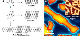 |
| (A) This image is a diagram of molecular precursors, the resulting graphene nanoribbons and the heterostructured ones. (B) Tunnel microscopy images of the heterostructures synthesized on gold surfaces.
CREDIT: UPV/EHU |
Abstract:
Few materials have received as much attention from the scientific world or have raised so many hopes with a view to their potential deployment in new applications as graphene has. This is largely due to its superlative properties: it is the thinnest material in existence, almost transparent, the strongest, the stiffest and at the same time the most strechable, the best thermal conductor, the one with the highest intrinsic charge carrier mobility, plus many more fascinating features. Specifically, its electronic properties can vary enormously through its confinement inside nanostructured systems, for example. That is why ribbons or rows of graphene with nanometric widths are emerging as tremendously interesting electronic components. On the other hand, due to the great variability of electronic properties upon minimal changes in the structure of these nanoribbons, exact control on an atomic level is an indispensable requirement to make the most of all their potential.
A new step towards using graphene in electronic applications
Alava, Spain | Posted on January 14th, 2015The lithographic techniques used in conventional nanotechnology do not yet have such resolution and precision. In the year 2010, however, a way was found to synthesise nanoribbons with atomic precision by means of the so-called molecular self-assembly. Molecules designed for this purpose are deposited onto a surface in such a way that they react with each other and give rise to perfectly specified graphene nanoribbons by means of a highly reproducible process and without any other external mediation than heating to the required temperature. In 2013 a team of scientists from the University of Berkeley and the Centre for Materials Physics (CFM), a mixed CSIC (Spanish National Research Council) and UPV/EHU (University of the Basque Country) centre, extended this very concept to new molecules that were forming wider graphene nanoribbons and therefore with new electronic properties. This same group has now managed to go a step further by creating, through this self-assembly, heterostructures that blend segments of graphene nanoribbons of two different widths.
The forming of heterostructures with different materials has been a concept widely used in electronic engineering and has enabled huge advances to be made in conventional electronics. "We have now managed for the first time to form heterostructures of graphene nanoribbons modulating their width on a molecular level with atomic precision. What is more, their subsequent characterisation by means of scanning tunnelling microscopy and spectroscopy, complemented with first principles theoretical calculations, has shown that it gives rise to a system with very interesting electronic properties which include, for example, the creation of what are known as quantum wells," pointed out the scientist Dimas de Oteyza, who has participated in this project. This work, the results of which are being published this very week in the prestigious journal Nature Nanotechnology, therefore constitutes a significant success towards the desired deployment of graphene in commercial electronic applications.
Dr Dimas G. de Oteyza, who was previously at Berkeley and at the CFM, is currently working at the Donostia International Physics Center (DIPC) as a Fellow Gipuzkoa. The Fellows Gipuzkoa programme, funded by the Chartered Provincial Council of Gipuzkoa, is in fact devoted to bringing back young researchers with solid post-doctoral training in internationally prestigious groups and centres, by offering them a platform for reincorporation through contracts with a duration of up to five years, which enables them to compete in the best of conditions to obtain tenured positions as researchers in our country.
####
For more information, please click here
Contacts:
Matxalen Sotillo
34-688-673-770
Copyright © University of the Basque Country
If you have a comment, please Contact us.Issuers of news releases, not 7th Wave, Inc. or Nanotechnology Now, are solely responsible for the accuracy of the content.
Bookmark:


| Related Links |
| Related News Press |
News and information
![]() Quantum computer improves AI predictions April 17th, 2026
Quantum computer improves AI predictions April 17th, 2026
![]() Flexible sensor gains sensitivity under pressure April 17th, 2026
Flexible sensor gains sensitivity under pressure April 17th, 2026
![]() A reusable chip for particulate matter sensing April 17th, 2026
A reusable chip for particulate matter sensing April 17th, 2026
![]() Detecting vibrational quantum beating in the predissociation dynamics of SF6 using time-resolved photoelectron spectroscopy April 17th, 2026
Detecting vibrational quantum beating in the predissociation dynamics of SF6 using time-resolved photoelectron spectroscopy April 17th, 2026
Graphene/ Graphite
![]() Electrifying results shed light on graphene foam as a potential material for lab grown cartilage June 6th, 2025
Electrifying results shed light on graphene foam as a potential material for lab grown cartilage June 6th, 2025
![]() Breakthrough in proton barrier films using pore-free graphene oxide: Kumamoto University researchers achieve new milestone in advanced coating technologies September 13th, 2024
Breakthrough in proton barrier films using pore-free graphene oxide: Kumamoto University researchers achieve new milestone in advanced coating technologies September 13th, 2024
Chip Technology
![]() A reusable chip for particulate matter sensing April 17th, 2026
A reusable chip for particulate matter sensing April 17th, 2026
![]() Metasurfaces smooth light to boost magnetic sensing precision January 30th, 2026
Metasurfaces smooth light to boost magnetic sensing precision January 30th, 2026
Nanoelectronics
![]() Lab to industry: InSe wafer-scale breakthrough for future electronics August 8th, 2025
Lab to industry: InSe wafer-scale breakthrough for future electronics August 8th, 2025
![]() Interdisciplinary: Rice team tackles the future of semiconductors Multiferroics could be the key to ultralow-energy computing October 6th, 2023
Interdisciplinary: Rice team tackles the future of semiconductors Multiferroics could be the key to ultralow-energy computing October 6th, 2023
![]() Key element for a scalable quantum computer: Physicists from Forschungszentrum J�lich and RWTH Aachen University demonstrate electron transport on a quantum chip September 23rd, 2022
Key element for a scalable quantum computer: Physicists from Forschungszentrum J�lich and RWTH Aachen University demonstrate electron transport on a quantum chip September 23rd, 2022
![]() Reduced power consumption in semiconductor devices September 23rd, 2022
Reduced power consumption in semiconductor devices September 23rd, 2022
Discoveries
![]() Quantum computer improves AI predictions April 17th, 2026
Quantum computer improves AI predictions April 17th, 2026
![]() Flexible sensor gains sensitivity under pressure April 17th, 2026
Flexible sensor gains sensitivity under pressure April 17th, 2026
![]() A reusable chip for particulate matter sensing April 17th, 2026
A reusable chip for particulate matter sensing April 17th, 2026
![]() Detecting vibrational quantum beating in the predissociation dynamics of SF6 using time-resolved photoelectron spectroscopy April 17th, 2026
Detecting vibrational quantum beating in the predissociation dynamics of SF6 using time-resolved photoelectron spectroscopy April 17th, 2026
Announcements
![]() A fundamentally new therapeutic approach to cystic fibrosis: Nanobody repairs cellular defect April 17th, 2026
A fundamentally new therapeutic approach to cystic fibrosis: Nanobody repairs cellular defect April 17th, 2026
![]() UC Irvine physicists discover method to reverse �quantum scrambling� : The work addresses the problem of information loss in quantum computing system April 17th, 2026
UC Irvine physicists discover method to reverse �quantum scrambling� : The work addresses the problem of information loss in quantum computing system April 17th, 2026
Interviews/Book Reviews/Essays/Reports/Podcasts/Journals/White papers/Posters
![]() A fundamentally new therapeutic approach to cystic fibrosis: Nanobody repairs cellular defect April 17th, 2026
A fundamentally new therapeutic approach to cystic fibrosis: Nanobody repairs cellular defect April 17th, 2026
![]() UC Irvine physicists discover method to reverse �quantum scrambling� : The work addresses the problem of information loss in quantum computing system April 17th, 2026
UC Irvine physicists discover method to reverse �quantum scrambling� : The work addresses the problem of information loss in quantum computing system April 17th, 2026
Printing/Lithography/Inkjet/Inks/Bio-printing/Dyes
![]() Presenting: Ultrasound-based printing of 3D materials�potentially inside the body December 8th, 2023
Presenting: Ultrasound-based printing of 3D materials�potentially inside the body December 8th, 2023
![]() Simple ballpoint pen can write custom LEDs August 11th, 2023
Simple ballpoint pen can write custom LEDs August 11th, 2023
![]() Disposable electronics on a simple sheet of paper October 7th, 2022
Disposable electronics on a simple sheet of paper October 7th, 2022
Quantum nanoscience
![]() Beyond silicon: Electronics at the scale of a single molecule January 30th, 2026
Beyond silicon: Electronics at the scale of a single molecule January 30th, 2026
![]() MXene nanomaterials enter a new dimension Multilayer nanomaterial: MXene flakes created at Drexel University show new promise as 1D scrolls January 30th, 2026
MXene nanomaterials enter a new dimension Multilayer nanomaterial: MXene flakes created at Drexel University show new promise as 1D scrolls January 30th, 2026
![]() ICFO researchers overcome long-standing bottleneck in single photon detection with twisted 2D materials August 8th, 2025
ICFO researchers overcome long-standing bottleneck in single photon detection with twisted 2D materials August 8th, 2025
|
|
||
|
|
||
| The latest news from around the world, FREE | ||
|
|
||
|
|
||
| Premium Products | ||
|
|
||
|
Only the news you want to read!
Learn More |
||
|
|
||
|
Full-service, expert consulting
Learn More |
||
|
|
||