Home > Press > High photosensitivity 2D-few-layered molybdenum diselenide phototransistors
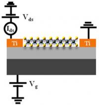 |
| This is the schematic structure of the few-layered MoSe2 FETs.
Credit: copyright (c) 2014 Toyohashi University of Technology. All rights reserved. |
Abstract:
Two-dimensional (2D) layered materials are now attracting a lot of interest due to their unique optoelectronic properties at atomic thicknesses. Among them, graphene has been mostly investigated, but the zero-gap nature of graphene limits its practical applications. Therefore, 2D layered materials with intrinsic band gaps such as MoS2, MoSe2, and MoTe2 are of interest as promising candidates for ultrathin and high-performance optoelectronic devices
High photosensitivity 2D-few-layered molybdenum diselenide phototransistors
Toyohashi, Japan | Posted on December 8th, 2014Here, Pil Ju Ko and colleagues at Toyohashi University of Technology, Japan have fabricated back-gated field-effect phototransistors made of MoSe2 crystals having a thickness of only twenty nanometers. The devices were fabricated by mechanical cleavage of MoSe2 crystals into few-layered flakes, followed by transfer onto a silicon wafer with pre-deposited titanium electrodes.
Despite their ultra-thin physical size, the devices showed excellent field-effect phototransistor characteristics. The measured photoresponsivity of 97.1 AW-1 at zero back gate voltage was higher than previous reports of photodetectors fabricated using GaS, GaSe, MoS2, and InSe. The photoresponse of the MoSe2 was much faster (less than 15 msec) than ultrasensitive photodetectors based on monolayer MoS2. Furthermore, the theoretical external quantum efficiency was 280-fold higher than of commercial Si and InGaAs photodiodes.
The research shows that MoSe2 is a promising material for photodetector applications. The group is optimization the device performance by studying thickness-dependent of the photosensitivity.
Reference:
Authors: Abdelkader Abderrahmane, Pil Ju Ko, Tran Viet Thu, Shunji Ishizawa, Tsukasa Takamura and Adarsh Sandhu.
Title of original paper: High photosensitivity few-layered MoSe2 back-gated field-effect phototransistors.
Journal, volume, pages and year: Nanotechnology 25 365202 (1-5) (2014).
Digital Object Identifier (DOI): 10.1088/0957-4484/25/36/365202.
Affiliations: Electronics-Inspired Interdisciplinary Research Institute (EIIRIS) and Department of Electrical and Electronic Information Engineering, Toyohashi University of Technology, 1-1 Hibarigaoka, Tempaku, Toyohashi, Aichi 441-8580, Japan
####
About Toyohashi University of Technology
Founded in 1976 as a National University of Japan, Toyohashi University of Technology is a vibrant modern institute with research activities reflecting the modern era of advanced electronics, engineering, and life sciences.
For more information, please click here
Contacts:
Toyohashi University of Technology
1-1 Hibarigaoka, Tempaku
Toyohashi, Aichi Prefecture, 441-8580, JAPAN
Inquiries: Committee for Public Relations
Michiteru Kitazaki
Copyright © Toyohashi University of Technology
If you have a comment, please Contact us.Issuers of news releases, not 7th Wave, Inc. or Nanotechnology Now, are solely responsible for the accuracy of the content.
Bookmark:


| Related Links |
| Related News Press |
News and information
![]() Quantum computer improves AI predictions April 17th, 2026
Quantum computer improves AI predictions April 17th, 2026
![]() Flexible sensor gains sensitivity under pressure April 17th, 2026
Flexible sensor gains sensitivity under pressure April 17th, 2026
![]() A reusable chip for particulate matter sensing April 17th, 2026
A reusable chip for particulate matter sensing April 17th, 2026
![]() Detecting vibrational quantum beating in the predissociation dynamics of SF6 using time-resolved photoelectron spectroscopy April 17th, 2026
Detecting vibrational quantum beating in the predissociation dynamics of SF6 using time-resolved photoelectron spectroscopy April 17th, 2026
Flexible Electronics
![]() Flexible sensor gains sensitivity under pressure April 17th, 2026
Flexible sensor gains sensitivity under pressure April 17th, 2026
![]() Flexible electronics integrated with paper-thin structure for use in space January 17th, 2025
Flexible electronics integrated with paper-thin structure for use in space January 17th, 2025
Display technology/LEDs/SS Lighting/OLEDs
![]() Spinel-type sulfide semiconductors to operate the next-generation LEDs and solar cells For solar-cell absorbers and green-LED source October 3rd, 2025
Spinel-type sulfide semiconductors to operate the next-generation LEDs and solar cells For solar-cell absorbers and green-LED source October 3rd, 2025
Graphene/ Graphite
![]() Electrifying results shed light on graphene foam as a potential material for lab grown cartilage June 6th, 2025
Electrifying results shed light on graphene foam as a potential material for lab grown cartilage June 6th, 2025
Chip Technology
![]() A reusable chip for particulate matter sensing April 17th, 2026
A reusable chip for particulate matter sensing April 17th, 2026
![]() Metasurfaces smooth light to boost magnetic sensing precision January 30th, 2026
Metasurfaces smooth light to boost magnetic sensing precision January 30th, 2026
Optical computing/Photonic computing
![]() ICFO researchers overcome long-standing bottleneck in single photon detection with twisted 2D materials August 8th, 2025
ICFO researchers overcome long-standing bottleneck in single photon detection with twisted 2D materials August 8th, 2025
![]() Programmable electron-induced color router array May 14th, 2025
Programmable electron-induced color router array May 14th, 2025
Discoveries
![]() Quantum computer improves AI predictions April 17th, 2026
Quantum computer improves AI predictions April 17th, 2026
![]() Flexible sensor gains sensitivity under pressure April 17th, 2026
Flexible sensor gains sensitivity under pressure April 17th, 2026
![]() A reusable chip for particulate matter sensing April 17th, 2026
A reusable chip for particulate matter sensing April 17th, 2026
![]() Detecting vibrational quantum beating in the predissociation dynamics of SF6 using time-resolved photoelectron spectroscopy April 17th, 2026
Detecting vibrational quantum beating in the predissociation dynamics of SF6 using time-resolved photoelectron spectroscopy April 17th, 2026
Announcements
![]() A fundamentally new therapeutic approach to cystic fibrosis: Nanobody repairs cellular defect April 17th, 2026
A fundamentally new therapeutic approach to cystic fibrosis: Nanobody repairs cellular defect April 17th, 2026
![]() UC Irvine physicists discover method to reverse �quantum scrambling� : The work addresses the problem of information loss in quantum computing system April 17th, 2026
UC Irvine physicists discover method to reverse �quantum scrambling� : The work addresses the problem of information loss in quantum computing system April 17th, 2026
Interviews/Book Reviews/Essays/Reports/Podcasts/Journals/White papers/Posters
![]() A fundamentally new therapeutic approach to cystic fibrosis: Nanobody repairs cellular defect April 17th, 2026
A fundamentally new therapeutic approach to cystic fibrosis: Nanobody repairs cellular defect April 17th, 2026
![]() UC Irvine physicists discover method to reverse �quantum scrambling� : The work addresses the problem of information loss in quantum computing system April 17th, 2026
UC Irvine physicists discover method to reverse �quantum scrambling� : The work addresses the problem of information loss in quantum computing system April 17th, 2026
Quantum nanoscience
![]() Beyond silicon: Electronics at the scale of a single molecule January 30th, 2026
Beyond silicon: Electronics at the scale of a single molecule January 30th, 2026
![]() MXene nanomaterials enter a new dimension Multilayer nanomaterial: MXene flakes created at Drexel University show new promise as 1D scrolls January 30th, 2026
MXene nanomaterials enter a new dimension Multilayer nanomaterial: MXene flakes created at Drexel University show new promise as 1D scrolls January 30th, 2026
![]() ICFO researchers overcome long-standing bottleneck in single photon detection with twisted 2D materials August 8th, 2025
ICFO researchers overcome long-standing bottleneck in single photon detection with twisted 2D materials August 8th, 2025
|
|
||
|
|
||
| The latest news from around the world, FREE | ||
|
|
||
|
|
||
| Premium Products | ||
|
|
||
|
Only the news you want to read!
Learn More |
||
|
|
||
|
Full-service, expert consulting
Learn More |
||
|
|
||