Home > Press > NRL Scientists Discover Novel Metamaterial Properties within Hexagonal Boron Nitride
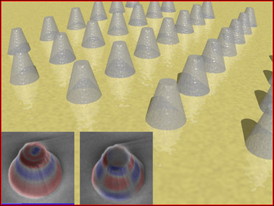 |
| Periodic arrays of cone-shaped hexagonal boron nitride (hBN) nanoantennas, depicted magnified image above, were used to confine hyperbolic polaritons in all three dimensions. This enabled the researchers to fundamentally probe the novel optical properties within these materials and demonstrate the highly directional, low loss hyperbolic polaritons that are confined within the volume of the antennas. These results provide the first foray into natural hyperbolic materials as building blocks for nanophotonic devices in the mid-infrared to terahertz (THz) spectral range.
Photo: U.S. Naval Research Laboratory |
Abstract:
U.S. Naval Research Laboratory (NRL) scientists, in collaboration with researchers from the University of Manchester, U.K.; Imperial College, London; University of California San Diego; and the National Institute of Material Science (NIMS), Japan, have demonstrated that confined surface phonon polaritons within hexagonal boron nitride (hBN) exhibit unique metamaterial properties that enable novel nanoscale optical devices for use in optical communications, super-resolution imaging, and improved infrared cameras and detectors.
NRL Scientists Discover Novel Metamaterial Properties within Hexagonal Boron Nitride
Washington, DC | Posted on November 20th, 2014Metamaterials are artificial composites of various materials designed to exhibit optical properties not anticipated in nature. One such property is hyperbolicity, whereby a material exhibits both metallic- and dielectric-like optical responses simultaneously along different crystal axes. These hyperbolic metamaterials are the basis for many potential applications such as 'hyperlenses,' used for imaging of nanoscale objects not observable using conventional optics.
"Our examination into the characteristics of hBN reveal the first experimental observation of sub-diffractional guided waves confined in all three dimensions, using a natural hyperbolic material," said Joshua Caldwell, Ph.D., Electronics Science and Technology Division, Power Electronics Branch. "This may, in turn, lead to the development of disruptive technologies such as the nanoscale equivalent of an optical fiber due to the volume-bound confinement of sub-diffractional modes within hBN."
Optic phonons, or crystal vibrations that can be excited with infrared light, can also be used to confine light to dimensions much smaller than the wavelength of light, while maintaining record-high efficiencies. These surface phonon polaritons are analogous to electron oscillations in metals or doped-semiconductors, called plasmons, but offer the benefit of low losses and operation in the infrared to terahertz spectral regions.
As a van der Waels crystal�a layered crystal structure similar to graphene or graphite�hBN was demonstrated to be two orders of magnitude more efficient than hyperbolic metamaterials shown to date, says Caldwell. Unlike metallic/dielectric hyperbolic metamaterials, hBN also provides the additional functionality of both types of hyperbolicity, allowing both the in-plane and out-of-plane crystal axes to behave metallic- (reflective) or dielectric-like (transparent) simply by changing the wavelength of the exciting light. This mixing of both types of hyperbolic behavior is to this point unique and allowed the fundamental comparison of antennas within these two regimes.
Using the natural hyperbolic behavior of hBN, the researchers were able to demonstrate that light could also be confined within optical antennas�up to 86 times smaller than the wavelength of light, for instance confinement of 6.8 micrometers of light into a 0.08 micrometer tall antenna�while maintaining record-high efficiencies due to the low-loss nature of the dielectric crystal.
The researchers were able to further demonstrate that the resonance wavelength of the hyperbolic polaritons confined within these antennae was dependent only upon the aspect ratio (height/diameter), and was nominally independent upon the actual size and/or shape�demonstrating that antennas could be defined for a given application simply by controlling this ratio, thereby making them compatible to a wide array of device form-factors. This could enable frequency selective operation and nanophotonic circuits, as well as provide an operational material for mid-infrared imaging of nanoscale objects.
The research team also demonstrated that the resonance response exhibited not a single mode, but four separate series, and according to Caldwell, a change in the wavelength and/or the angle of the incoming light with respect to the sample surface could isolate each series, providing the first complete description of these novel, three-dimensionally confined hyperbolic polariton modes.
Further discoveries found these breakthroughs could have an impact in areas such as enhanced infrared or molecular spectroscopy, improved functionality for nanophotonic circuits and devices for use in infrared cameras, detectors and weapons guidance systems, and tailored thermal emission sources.
The NRL Power Electronics Branch serves as the laboratory's principal resource for the science and technology of solid-state high-power electronic devices. The primary mission of the branch is to conduct research and development (R&D) programs in solid state electronics and related technologies that support U.S. Navy and Department of Defense (DoD) interests and capabilities in the full range of new weapons capabilities enabled by high-power solid state electronic devices. Moreover, the branch serves as the focal point of insertion of power electronics technology into Navy engineering development efforts.
####
About Naval Research Laboratory
The U.S. Naval Research Laboratory is the Navy's full-spectrum corporate laboratory, conducting a broadly based multidisciplinary program of scientific research and advanced technological development. The Laboratory, with a total complement of approximately 2,500 personnel, is located in southwest Washington, D.C., with other major sites at the Stennis Space Center, Miss., and Monterey, Calif. NRL has served the Navy and the nation for over 90 years and continues to meet the complex technological challenges of today's world. For more information, visit the NRL homepage or join the conversation on Twitter, Facebook, and YouTube.
For more information, please click here
Contacts:
Daniel Parry
202-767-2541
Copyright © Naval Research Laboratory
If you have a comment, please Contact us.Issuers of news releases, not 7th Wave, Inc. or Nanotechnology Now, are solely responsible for the accuracy of the content.
Bookmark:


| Related News Press |
News and information
![]() Quantum computer improves AI predictions April 17th, 2026
Quantum computer improves AI predictions April 17th, 2026
![]() Flexible sensor gains sensitivity under pressure April 17th, 2026
Flexible sensor gains sensitivity under pressure April 17th, 2026
![]() A reusable chip for particulate matter sensing April 17th, 2026
A reusable chip for particulate matter sensing April 17th, 2026
![]() Detecting vibrational quantum beating in the predissociation dynamics of SF6 using time-resolved photoelectron spectroscopy April 17th, 2026
Detecting vibrational quantum beating in the predissociation dynamics of SF6 using time-resolved photoelectron spectroscopy April 17th, 2026
Imaging
![]() Simple algorithm paired with standard imaging tool could predict failure in lithium metal batteries August 8th, 2025
Simple algorithm paired with standard imaging tool could predict failure in lithium metal batteries August 8th, 2025
![]() First real-time observation of two-dimensional melting process: Researchers at Mainz University unveil new insights into magnetic vortex structures August 8th, 2025
First real-time observation of two-dimensional melting process: Researchers at Mainz University unveil new insights into magnetic vortex structures August 8th, 2025
![]() New imaging approach transforms study of bacterial biofilms August 8th, 2025
New imaging approach transforms study of bacterial biofilms August 8th, 2025
Laboratories
![]() Researchers develop molecular qubits that communicate at telecom frequencies October 3rd, 2025
Researchers develop molecular qubits that communicate at telecom frequencies October 3rd, 2025
Wireless/telecommunications/RF/Antennas/Microwaves
![]() Researchers develop molecular qubits that communicate at telecom frequencies October 3rd, 2025
Researchers develop molecular qubits that communicate at telecom frequencies October 3rd, 2025
Govt.-Legislation/Regulation/Funding/Policy
![]() Quantum computer improves AI predictions April 17th, 2026
Quantum computer improves AI predictions April 17th, 2026
![]() Metasurfaces smooth light to boost magnetic sensing precision January 30th, 2026
Metasurfaces smooth light to boost magnetic sensing precision January 30th, 2026
![]() New imaging approach transforms study of bacterial biofilms August 8th, 2025
New imaging approach transforms study of bacterial biofilms August 8th, 2025
Discoveries
![]() Quantum computer improves AI predictions April 17th, 2026
Quantum computer improves AI predictions April 17th, 2026
![]() Flexible sensor gains sensitivity under pressure April 17th, 2026
Flexible sensor gains sensitivity under pressure April 17th, 2026
![]() A reusable chip for particulate matter sensing April 17th, 2026
A reusable chip for particulate matter sensing April 17th, 2026
![]() Detecting vibrational quantum beating in the predissociation dynamics of SF6 using time-resolved photoelectron spectroscopy April 17th, 2026
Detecting vibrational quantum beating in the predissociation dynamics of SF6 using time-resolved photoelectron spectroscopy April 17th, 2026
Announcements
![]() A fundamentally new therapeutic approach to cystic fibrosis: Nanobody repairs cellular defect April 17th, 2026
A fundamentally new therapeutic approach to cystic fibrosis: Nanobody repairs cellular defect April 17th, 2026
![]() UC Irvine physicists discover method to reverse �quantum scrambling� : The work addresses the problem of information loss in quantum computing system April 17th, 2026
UC Irvine physicists discover method to reverse �quantum scrambling� : The work addresses the problem of information loss in quantum computing system April 17th, 2026
Interviews/Book Reviews/Essays/Reports/Podcasts/Journals/White papers/Posters
![]() A fundamentally new therapeutic approach to cystic fibrosis: Nanobody repairs cellular defect April 17th, 2026
A fundamentally new therapeutic approach to cystic fibrosis: Nanobody repairs cellular defect April 17th, 2026
![]() UC Irvine physicists discover method to reverse �quantum scrambling� : The work addresses the problem of information loss in quantum computing system April 17th, 2026
UC Irvine physicists discover method to reverse �quantum scrambling� : The work addresses the problem of information loss in quantum computing system April 17th, 2026
Military
![]() Quantum engineers �squeeze� laser frequency combs to make more sensitive gas sensors January 17th, 2025
Quantum engineers �squeeze� laser frequency combs to make more sensitive gas sensors January 17th, 2025
![]() Chainmail-like material could be the future of armor: First 2D mechanically interlocked polymer exhibits exceptional flexibility and strength January 17th, 2025
Chainmail-like material could be the future of armor: First 2D mechanically interlocked polymer exhibits exceptional flexibility and strength January 17th, 2025
![]() Single atoms show their true color July 5th, 2024
Single atoms show their true color July 5th, 2024
![]() NRL charters Navy�s quantum inertial navigation path to reduce drift April 5th, 2024
NRL charters Navy�s quantum inertial navigation path to reduce drift April 5th, 2024
Photonics/Optics/Lasers
![]() Metasurfaces smooth light to boost magnetic sensing precision January 30th, 2026
Metasurfaces smooth light to boost magnetic sensing precision January 30th, 2026
![]() From sensors to smart systems: the rise of AI-driven photonic noses January 30th, 2026
From sensors to smart systems: the rise of AI-driven photonic noses January 30th, 2026
Research partnerships
![]() Lab to industry: InSe wafer-scale breakthrough for future electronics August 8th, 2025
Lab to industry: InSe wafer-scale breakthrough for future electronics August 8th, 2025
![]() HKU physicists uncover hidden order in the quantum world through deconfined quantum critical points April 25th, 2025
HKU physicists uncover hidden order in the quantum world through deconfined quantum critical points April 25th, 2025
|
|
||
|
|
||
| The latest news from around the world, FREE | ||
|
|
||
|
|
||
| Premium Products | ||
|
|
||
|
Only the news you want to read!
Learn More |
||
|
|
||
|
Full-service, expert consulting
Learn More |
||
|
|
||