Home > Press > 'Direct writing' of diamond patterns from graphite a potential technological leap
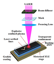 |
| This illustration depicts a new technique that uses a pulsing laser to create synthetic nanodiamond films and patterns from graphite, with potential applications from biosensors to computer chips. Purdue University image/Gary Cheng |
Abstract:
Direct Laser Writing of Nanodiamond Films from Graphite under Ambient Conditions
Qiong Nian, Yuefeng Wang, Yingling Yang, Ji Li, Martin Y. Zhang, Jiayi Shao, Liang Tang & Gary J. Cheng
Purdue University
Synthesis of diamond, a multi-functional material, has been a challenge due to very high activation energy for transforming graphite to diamond, and therefore, has been hindering it from being potentially exploited for novel applications. In this study, we explore a new approach, namely confined pulse laser deposition (CPLD), in which nanosecond laser ablation of graphite within a confinement layer simultaneously activates plasma and effectively confine it to create a favorable condition for nanodiamond formation from graphite. It is noteworthy that due to the local high dense confined plasma created by transparent confinement layer, nanodiamond has been formed at laser intensity as low as 3.7 GW/cm2, which corresponds to pressure of 4.4 GPa, much lower than the pressure needed to transform graphite to diamond traditionally. By manipulating the laser conditions, semi-transparent carbon films with good conductivity (several kΩ/Sq) were also obtained by this method. This technique provides a new channel, from confined plasma to solid, to deposit materials that normally need high temperature and high pressure. This technique has several important advantages to allow scalable processing, such as high speed, direct writing without catalyst, selective and flexible processing, low cost without expensive pico/femtosecond laser systems, high temperature/vacuum chambers.
'Direct writing' of diamond patterns from graphite a potential technological leap
West Lafayette, IN | Posted on November 5th, 2014What began as research into a method to strengthen metals has led to the discovery of a new technique that uses a pulsing laser to create synthetic nanodiamond films and patterns from graphite, with potential applications from biosensors to computer chips.
"The biggest advantage is that you can selectively deposit nanodiamond on rigid surfaces without the high temperatures and pressures normally needed to produce synthetic diamond," said Gary Cheng, an associate professor of industrial engineering at Purdue University. "We do this at room temperature and without a high temperature and pressure chamber, so this process could significantly lower the cost of making diamond. In addition, we realize a direct writing technique that could selectively write nanodiamond in designed patterns."
The ability to selectively "write" lines of diamond on surfaces could be practical for various potential applications including biosensors, quantum computing, fuel cells and next-generation computer chips.
The technique works by using a multilayered film that includes a layer of graphite topped with a glass cover sheet. Exposing this layered structure to an ultrafast-pulsing laser instantly converts the graphite to an ionized plasma and creates a downward pressure. Then the graphite plasma quickly solidifies into diamond. The glass sheet confines the plasma to keep it from escaping, allowing it to form a nanodiamond coating.
"These are super-small diamonds and the coating is super-strong, so it could be used for high-temperature sensors," Cheng said.
Research findings are detailed in a paper that appeared online in the Nature journal Scientific Reports. The paper was authored by former Purdue doctoral students Yuefeng Wang, Yingling Yang, Ji Li and Martin Y. Zhang; postdoctoral research associate Jiayi Shao; doctoral students Qiong Nian and Liang Tang; and Cheng.
The researchers made the discovery while studying how to strengthen metals using a thin layer of graphite and a nanosecond-pulsing laser. A doctoral student noticed that the laser was either causing the graphite to disappear or turn semi-transparent.
"The black coating of graphite was gone, but where did it go?" Cheng said.
Subsequent research proved the graphite had turned into diamond. The Purdue researchers have named the process confined pulse laser deposition (CPLD).
The research team confirmed that the structures are diamond using a variety of techniques including transmission electron microscopy, X-ray diffraction and the measurement of electrical resistance.
A U.S. patent application has been filed on the concept through the Purdue Office of Technology Commercialization. More research is needed to commercialize the technique, Cheng said.
####
For more information, please click here
Contacts:
Writer:
Emil Venere
765-494-4709
Source:
Gary J. Cheng
765-494-5436
Copyright © Purdue University
If you have a comment, please Contact us.Issuers of news releases, not 7th Wave, Inc. or Nanotechnology Now, are solely responsible for the accuracy of the content.
Bookmark:


| Related News Press |
News and information
![]() Quantum computer improves AI predictions April 17th, 2026
Quantum computer improves AI predictions April 17th, 2026
![]() Flexible sensor gains sensitivity under pressure April 17th, 2026
Flexible sensor gains sensitivity under pressure April 17th, 2026
![]() A reusable chip for particulate matter sensing April 17th, 2026
A reusable chip for particulate matter sensing April 17th, 2026
![]() Detecting vibrational quantum beating in the predissociation dynamics of SF6 using time-resolved photoelectron spectroscopy April 17th, 2026
Detecting vibrational quantum beating in the predissociation dynamics of SF6 using time-resolved photoelectron spectroscopy April 17th, 2026
Thin films
![]() Tiny nanosheets, big leap: A new sensor detects ethanol at ultra-low levels January 30th, 2026
Tiny nanosheets, big leap: A new sensor detects ethanol at ultra-low levels January 30th, 2026
![]() Utilizing palladium for addressing contact issues of buried oxide thin film transistors April 5th, 2024
Utilizing palladium for addressing contact issues of buried oxide thin film transistors April 5th, 2024
![]() Understanding the mechanism of non-uniform formation of diamond film on tools: Paving the way to a dry process with less environmental impact March 24th, 2023
Understanding the mechanism of non-uniform formation of diamond film on tools: Paving the way to a dry process with less environmental impact March 24th, 2023
![]() New study introduces the best graphite films: The work by Distinguished Professor Feng Ding at UNIST has been published in the October 2022 issue of Nature Nanotechnology November 4th, 2022
New study introduces the best graphite films: The work by Distinguished Professor Feng Ding at UNIST has been published in the October 2022 issue of Nature Nanotechnology November 4th, 2022
Chip Technology
![]() A reusable chip for particulate matter sensing April 17th, 2026
A reusable chip for particulate matter sensing April 17th, 2026
![]() Metasurfaces smooth light to boost magnetic sensing precision January 30th, 2026
Metasurfaces smooth light to boost magnetic sensing precision January 30th, 2026
Sensors
![]() Flexible sensor gains sensitivity under pressure April 17th, 2026
Flexible sensor gains sensitivity under pressure April 17th, 2026
![]() Tiny nanosheets, big leap: A new sensor detects ethanol at ultra-low levels January 30th, 2026
Tiny nanosheets, big leap: A new sensor detects ethanol at ultra-low levels January 30th, 2026
![]() From sensors to smart systems: the rise of AI-driven photonic noses January 30th, 2026
From sensors to smart systems: the rise of AI-driven photonic noses January 30th, 2026
![]() Sensors innovations for smart lithium-based batteries: advancements, opportunities, and potential challenges August 8th, 2025
Sensors innovations for smart lithium-based batteries: advancements, opportunities, and potential challenges August 8th, 2025
Discoveries
![]() Quantum computer improves AI predictions April 17th, 2026
Quantum computer improves AI predictions April 17th, 2026
![]() Flexible sensor gains sensitivity under pressure April 17th, 2026
Flexible sensor gains sensitivity under pressure April 17th, 2026
![]() A reusable chip for particulate matter sensing April 17th, 2026
A reusable chip for particulate matter sensing April 17th, 2026
![]() Detecting vibrational quantum beating in the predissociation dynamics of SF6 using time-resolved photoelectron spectroscopy April 17th, 2026
Detecting vibrational quantum beating in the predissociation dynamics of SF6 using time-resolved photoelectron spectroscopy April 17th, 2026
Materials/Metamaterials/Magnetoresistance
![]() First real-time observation of two-dimensional melting process: Researchers at Mainz University unveil new insights into magnetic vortex structures August 8th, 2025
First real-time observation of two-dimensional melting process: Researchers at Mainz University unveil new insights into magnetic vortex structures August 8th, 2025
![]() Researchers unveil a groundbreaking clay-based solution to capture carbon dioxide and combat climate change June 6th, 2025
Researchers unveil a groundbreaking clay-based solution to capture carbon dioxide and combat climate change June 6th, 2025
![]() A 1960s idea inspires NBI researchers to study hitherto inaccessible quantum states June 6th, 2025
A 1960s idea inspires NBI researchers to study hitherto inaccessible quantum states June 6th, 2025
![]() Institute for Nanoscience hosts annual proposal planning meeting May 16th, 2025
Institute for Nanoscience hosts annual proposal planning meeting May 16th, 2025
Announcements
![]() A fundamentally new therapeutic approach to cystic fibrosis: Nanobody repairs cellular defect April 17th, 2026
A fundamentally new therapeutic approach to cystic fibrosis: Nanobody repairs cellular defect April 17th, 2026
![]() UC Irvine physicists discover method to reverse �quantum scrambling� : The work addresses the problem of information loss in quantum computing system April 17th, 2026
UC Irvine physicists discover method to reverse �quantum scrambling� : The work addresses the problem of information loss in quantum computing system April 17th, 2026
Interviews/Book Reviews/Essays/Reports/Podcasts/Journals/White papers/Posters
![]() A fundamentally new therapeutic approach to cystic fibrosis: Nanobody repairs cellular defect April 17th, 2026
A fundamentally new therapeutic approach to cystic fibrosis: Nanobody repairs cellular defect April 17th, 2026
![]() UC Irvine physicists discover method to reverse �quantum scrambling� : The work addresses the problem of information loss in quantum computing system April 17th, 2026
UC Irvine physicists discover method to reverse �quantum scrambling� : The work addresses the problem of information loss in quantum computing system April 17th, 2026
Tools
![]() Metasurfaces smooth light to boost magnetic sensing precision January 30th, 2026
Metasurfaces smooth light to boost magnetic sensing precision January 30th, 2026
![]() From sensors to smart systems: the rise of AI-driven photonic noses January 30th, 2026
From sensors to smart systems: the rise of AI-driven photonic noses January 30th, 2026
![]() Japan launches fully domestically produced quantum computer: Expo visitors to experience quantum computing firsthand August 8th, 2025
Japan launches fully domestically produced quantum computer: Expo visitors to experience quantum computing firsthand August 8th, 2025
Patents/IP/Tech Transfer/Licensing
![]() Getting drugs across the blood-brain barrier using nanoparticles March 3rd, 2023
Getting drugs across the blood-brain barrier using nanoparticles March 3rd, 2023
![]() Metasurfaces control polarized light at will: New research unlocks the hidden potential of metasurfaces August 13th, 2021
Metasurfaces control polarized light at will: New research unlocks the hidden potential of metasurfaces August 13th, 2021
![]() Arrowhead Pharmaceuticals Announces Closing of Agreement with Takeda November 27th, 2020
Arrowhead Pharmaceuticals Announces Closing of Agreement with Takeda November 27th, 2020
Photonics/Optics/Lasers
![]() Metasurfaces smooth light to boost magnetic sensing precision January 30th, 2026
Metasurfaces smooth light to boost magnetic sensing precision January 30th, 2026
![]() From sensors to smart systems: the rise of AI-driven photonic noses January 30th, 2026
From sensors to smart systems: the rise of AI-driven photonic noses January 30th, 2026
|
|
||
|
|
||
| The latest news from around the world, FREE | ||
|
|
||
|
|
||
| Premium Products | ||
|
|
||
|
Only the news you want to read!
Learn More |
||
|
|
||
|
Full-service, expert consulting
Learn More |
||
|
|
||