Home > Press > Fast, cheap nanomanufacturing: Arrays of tiny conical tips that eject ionized materials could fabricate nanoscale devices cheaply
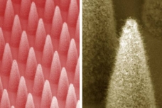 |
| At left is a dense array of electrospray emitters (1,900 emitters in 1 centimeter square). At right is a close-up of a single emitter, covered by a forest of carbon nanotubes.
Image: Journal of Micrelectromechanical Systems/colorized by MIT News |
Abstract:
Luis Fernando Velásquez-García's group at MIT's Microsystems Technology Laboratories (MTL) develops dense arrays of microscopic cones that harness electrostatic forces to eject streams of ions.
Fast, cheap nanomanufacturing: Arrays of tiny conical tips that eject ionized materials could fabricate nanoscale devices cheaply
Cambridge, MA | Posted on October 4th, 2014The technology has a range of promising applications: depositing or etching features onto nanoscale mechanical devices; spinning out nanofibers for use in water filters, body armor, and "smart" textiles; or propulsion systems for fist-sized "nanosatellites."
In the latest issue of the IEEE Journal of Microelectromechanical Systems, Velásquez-García, his graduate students Eric Heubel and Philip Ponce de Leon, and Frances Hill, a postdoc in his group, describe a new prototype array that generates 10 times the ion current per emitter that previous arrays did.
Ion current is a measure of the charge carried by moving ions, which translates directly to the rate at which particles can be ejected. Higher currents thus promise more-efficient manufacturing and more-nimble satellites.
The same prototype also crams 1,900 emitters onto a chip that's only a centimeter square, quadrupling the array size and emitter density of even the best of its predecessors.
"This is a field that benefits from miniaturizing the components, because scaling down emitters implies less power consumption, less bias voltage to operate them, and higher throughput," says Velásquez-García, a principal research scientist at MTL. "The topic we have been tackling is how we can make these devices operate as close as we can to the theoretical limit and how we can greatly increase the throughput by virtue of multiplexing, with massively parallel devices that operate uniformly."
When Velásquez-García speaks of a "theoretical limit," he's talking about the point at which droplets — clumps of molecules — rather than ions — individual molecules — begin streaming off of the emitters. Among other problems, droplets are heavier, so their ejection velocity is lower, which makes them less useful for etching or satellite propulsion.
The ions ejected by Velásquez-García's prototype are produced from an ionic salt that's liquid at room temperature. Surface tension wicks the fluid up the side of the emitters to the tip of the cone, whose narrowness concentrates the electrostatic field. At the tip, the liquid is ionized and, ideally, ejected one molecule at a time.
Slow the Flow
When the ion current in an emitter gets high enough, droplet formation is inevitable. But earlier emitter arrays — those built both by Velásquez-García's group and by others — fell well short of that threshold.
Increasing an array's ion current is a matter of regulating the flow of the ionic salt up the emitters' sides. To do that, the MIT researchers had previously used black silicon, a form of silicon grown as closely packed bristles. But in the new work, they instead used carbon nanotubes — atom-thick sheets of carbon rolled into cylinders — grown on the slopes of the emitters like trees on a mountainside.
By carefully tailoring the density and height of the nanotubes, the researchers were able to achieve a fluid flow that enabled an operating ion current at very near the theoretical limit.
"We also show that they work uniformly — that each emitter is doing exactly the same thing," Velásquez-García says. That's crucial for nanofabrication applications, in which the depth of an etch, or the height of deposits, must be consistent across an entire chip.
To control the nanotubes' growth, the researchers first cover the emitter array with an ultrathin catalyst film, which is broken into particles by chemical reactions with both the substrate and the environment. Then they expose the array to a plasma rich in carbon. The nanotubes grow up under the catalyst particles, which sit atop them, until the catalyst degrades.
Increasing the emitter density — the other improvement reported in the new paper — was a matter of optimizing existing manufacturing "recipe," Velásquez-García says. The emitters, like most nanoscale silicon devices, were produced through photolithography, a process in which patterns are optically transferred to layers of materials deposited on silicon wafers; a plasma then etches the material away according to the pattern. "The recipe is the gases, power, pressure level, time, and the sequence of the etching," Velásquez-García says. "We started doing electrospray arrays 15 years ago, and making different generations of devices gave us the know-how to make them better."
Nanoprinting
Velásquez-García believes that using arrays of emitters to produce nanodevices could have several advantages over photolithography — the technique that produces the arrays themselves. Because they can operate at room temperature and don't require a vacuum chamber, the arrays could deposit materials that can't withstand the extreme conditions of many micro- and nanomanufacturing processes. And they could eliminate the time-consuming process of depositing new layers of material, exposing them to optical patterns, etching them, and then starting all over again.
"In my opinion, the best nanosystems are going to be done by 3-D printing because it would bypass the problems of standard microfabrication," Velásquez-García says. "It uses prohibitively expensive equipment, which requires a high level of training to operate, and everything is defined in planes. In many applications you want the three-dimensionality: 3-D printing is going to make a big difference in the kinds of systems we can put together and the optimization that we can do."
Written by Larry Hardesty, MIT News Office.
####
For more information, please click here
Contacts:
Abby Abazorius
617-253-2709
Copyright © Massachusetts Institute of Technology
If you have a comment, please Contact us.Issuers of news releases, not 7th Wave, Inc. or Nanotechnology Now, are solely responsible for the accuracy of the content.
Bookmark:


| Related Links |
![]() Making 'nanospinning' practical:
Making 'nanospinning' practical:
![]() How to corner the MEMS market:
How to corner the MEMS market:
| Related News Press |
News and information
![]() Quantum computer improves AI predictions April 17th, 2026
Quantum computer improves AI predictions April 17th, 2026
![]() Flexible sensor gains sensitivity under pressure April 17th, 2026
Flexible sensor gains sensitivity under pressure April 17th, 2026
![]() A reusable chip for particulate matter sensing April 17th, 2026
A reusable chip for particulate matter sensing April 17th, 2026
![]() Detecting vibrational quantum beating in the predissociation dynamics of SF6 using time-resolved photoelectron spectroscopy April 17th, 2026
Detecting vibrational quantum beating in the predissociation dynamics of SF6 using time-resolved photoelectron spectroscopy April 17th, 2026
3D & 4D printing/Additive-manufacturing
![]() Presenting: Ultrasound-based printing of 3D materials—potentially inside the body December 8th, 2023
Presenting: Ultrasound-based printing of 3D materials—potentially inside the body December 8th, 2023
![]() Fiber sensing scientists invent 3D printed fiber microprobe for measuring in vivo biomechanical properties of tissue and even single cell February 10th, 2023
Fiber sensing scientists invent 3D printed fiber microprobe for measuring in vivo biomechanical properties of tissue and even single cell February 10th, 2023
![]() 3D-printed decoder, AI-enabled image compression could enable higher-res displays December 9th, 2022
3D-printed decoder, AI-enabled image compression could enable higher-res displays December 9th, 2022
![]() Researchers design new inks for 3D-printable wearable bioelectronics: Potential uses include printing electronic tattoos for medical tracking applications August 19th, 2022
Researchers design new inks for 3D-printable wearable bioelectronics: Potential uses include printing electronic tattoos for medical tracking applications August 19th, 2022
Govt.-Legislation/Regulation/Funding/Policy
![]() Quantum computer improves AI predictions April 17th, 2026
Quantum computer improves AI predictions April 17th, 2026
![]() Metasurfaces smooth light to boost magnetic sensing precision January 30th, 2026
Metasurfaces smooth light to boost magnetic sensing precision January 30th, 2026
![]() New imaging approach transforms study of bacterial biofilms August 8th, 2025
New imaging approach transforms study of bacterial biofilms August 8th, 2025
Molecular Nanotechnology
![]() Quantum pumping in molecular junctions August 16th, 2024
Quantum pumping in molecular junctions August 16th, 2024
![]() Scientists push the boundaries of manipulating light at the submicroscopic level March 3rd, 2023
Scientists push the boundaries of manipulating light at the submicroscopic level March 3rd, 2023
![]() First electric nanomotor made from DNA material: Synthetic rotary motors at the nanoscale perform mechanical work July 22nd, 2022
First electric nanomotor made from DNA material: Synthetic rotary motors at the nanoscale perform mechanical work July 22nd, 2022
Chip Technology
![]() A reusable chip for particulate matter sensing April 17th, 2026
A reusable chip for particulate matter sensing April 17th, 2026
![]() Metasurfaces smooth light to boost magnetic sensing precision January 30th, 2026
Metasurfaces smooth light to boost magnetic sensing precision January 30th, 2026
Nanotubes/Buckyballs/Fullerenes/Nanorods/Nanostrings/Nanosheets
![]() Tiny nanosheets, big leap: A new sensor detects ethanol at ultra-low levels January 30th, 2026
Tiny nanosheets, big leap: A new sensor detects ethanol at ultra-low levels January 30th, 2026
![]() Enhancing power factor of p- and n-type single-walled carbon nanotubes April 25th, 2025
Enhancing power factor of p- and n-type single-walled carbon nanotubes April 25th, 2025
![]() Chainmail-like material could be the future of armor: First 2D mechanically interlocked polymer exhibits exceptional flexibility and strength January 17th, 2025
Chainmail-like material could be the future of armor: First 2D mechanically interlocked polymer exhibits exceptional flexibility and strength January 17th, 2025
![]() Innovative biomimetic superhydrophobic coating combines repair and buffering properties for superior anti-erosion December 13th, 2024
Innovative biomimetic superhydrophobic coating combines repair and buffering properties for superior anti-erosion December 13th, 2024
Nanoelectronics
![]() Lab to industry: InSe wafer-scale breakthrough for future electronics August 8th, 2025
Lab to industry: InSe wafer-scale breakthrough for future electronics August 8th, 2025
![]() Interdisciplinary: Rice team tackles the future of semiconductors Multiferroics could be the key to ultralow-energy computing October 6th, 2023
Interdisciplinary: Rice team tackles the future of semiconductors Multiferroics could be the key to ultralow-energy computing October 6th, 2023
![]() Key element for a scalable quantum computer: Physicists from Forschungszentrum Jülich and RWTH Aachen University demonstrate electron transport on a quantum chip September 23rd, 2022
Key element for a scalable quantum computer: Physicists from Forschungszentrum Jülich and RWTH Aachen University demonstrate electron transport on a quantum chip September 23rd, 2022
![]() Reduced power consumption in semiconductor devices September 23rd, 2022
Reduced power consumption in semiconductor devices September 23rd, 2022
Discoveries
![]() Quantum computer improves AI predictions April 17th, 2026
Quantum computer improves AI predictions April 17th, 2026
![]() Flexible sensor gains sensitivity under pressure April 17th, 2026
Flexible sensor gains sensitivity under pressure April 17th, 2026
![]() A reusable chip for particulate matter sensing April 17th, 2026
A reusable chip for particulate matter sensing April 17th, 2026
![]() Detecting vibrational quantum beating in the predissociation dynamics of SF6 using time-resolved photoelectron spectroscopy April 17th, 2026
Detecting vibrational quantum beating in the predissociation dynamics of SF6 using time-resolved photoelectron spectroscopy April 17th, 2026
Materials/Metamaterials/Magnetoresistance
![]() First real-time observation of two-dimensional melting process: Researchers at Mainz University unveil new insights into magnetic vortex structures August 8th, 2025
First real-time observation of two-dimensional melting process: Researchers at Mainz University unveil new insights into magnetic vortex structures August 8th, 2025
![]() Researchers unveil a groundbreaking clay-based solution to capture carbon dioxide and combat climate change June 6th, 2025
Researchers unveil a groundbreaking clay-based solution to capture carbon dioxide and combat climate change June 6th, 2025
![]() A 1960s idea inspires NBI researchers to study hitherto inaccessible quantum states June 6th, 2025
A 1960s idea inspires NBI researchers to study hitherto inaccessible quantum states June 6th, 2025
![]() Institute for Nanoscience hosts annual proposal planning meeting May 16th, 2025
Institute for Nanoscience hosts annual proposal planning meeting May 16th, 2025
Announcements
![]() A fundamentally new therapeutic approach to cystic fibrosis: Nanobody repairs cellular defect April 17th, 2026
A fundamentally new therapeutic approach to cystic fibrosis: Nanobody repairs cellular defect April 17th, 2026
![]() UC Irvine physicists discover method to reverse ‘quantum scrambling’ : The work addresses the problem of information loss in quantum computing system April 17th, 2026
UC Irvine physicists discover method to reverse ‘quantum scrambling’ : The work addresses the problem of information loss in quantum computing system April 17th, 2026
Interviews/Book Reviews/Essays/Reports/Podcasts/Journals/White papers/Posters
![]() A fundamentally new therapeutic approach to cystic fibrosis: Nanobody repairs cellular defect April 17th, 2026
A fundamentally new therapeutic approach to cystic fibrosis: Nanobody repairs cellular defect April 17th, 2026
![]() UC Irvine physicists discover method to reverse ‘quantum scrambling’ : The work addresses the problem of information loss in quantum computing system April 17th, 2026
UC Irvine physicists discover method to reverse ‘quantum scrambling’ : The work addresses the problem of information loss in quantum computing system April 17th, 2026
Military
![]() Quantum engineers ‘squeeze’ laser frequency combs to make more sensitive gas sensors January 17th, 2025
Quantum engineers ‘squeeze’ laser frequency combs to make more sensitive gas sensors January 17th, 2025
![]() Chainmail-like material could be the future of armor: First 2D mechanically interlocked polymer exhibits exceptional flexibility and strength January 17th, 2025
Chainmail-like material could be the future of armor: First 2D mechanically interlocked polymer exhibits exceptional flexibility and strength January 17th, 2025
![]() Single atoms show their true color July 5th, 2024
Single atoms show their true color July 5th, 2024
![]() NRL charters Navy’s quantum inertial navigation path to reduce drift April 5th, 2024
NRL charters Navy’s quantum inertial navigation path to reduce drift April 5th, 2024
Water
![]() Taking salt out of the water equation October 7th, 2022
Taking salt out of the water equation October 7th, 2022
Aerospace/Space
![]() Decoding hydrogen‑bond network of electrolyte for cryogenic durable aqueous zinc‑ion batteries January 30th, 2026
Decoding hydrogen‑bond network of electrolyte for cryogenic durable aqueous zinc‑ion batteries January 30th, 2026
![]() ICFO researchers overcome long-standing bottleneck in single photon detection with twisted 2D materials August 8th, 2025
ICFO researchers overcome long-standing bottleneck in single photon detection with twisted 2D materials August 8th, 2025
![]() Onion-like nanoparticles found in aircraft exhaust May 14th, 2025
Onion-like nanoparticles found in aircraft exhaust May 14th, 2025
Printing/Lithography/Inkjet/Inks/Bio-printing/Dyes
![]() Presenting: Ultrasound-based printing of 3D materials—potentially inside the body December 8th, 2023
Presenting: Ultrasound-based printing of 3D materials—potentially inside the body December 8th, 2023
![]() Simple ballpoint pen can write custom LEDs August 11th, 2023
Simple ballpoint pen can write custom LEDs August 11th, 2023
![]() Disposable electronics on a simple sheet of paper October 7th, 2022
Disposable electronics on a simple sheet of paper October 7th, 2022
|
|
||
|
|
||
| The latest news from around the world, FREE | ||
|
|
||
|
|
||
| Premium Products | ||
|
|
||
|
Only the news you want to read!
Learn More |
||
|
|
||
|
Full-service, expert consulting
Learn More |
||
|
|
||