Home > Press > Material development on the nanoscale: Doped graphene nanoribbons with potential
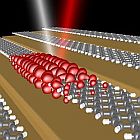 |
| Unlike graphene, which shows a wavelength-independent absorbance for visible light, light absorption can be increased enormously in a controlled way with graphene nanoribbons. This is achieved by setting the width of the graphene nanoribbons with atomic precision. |
Abstract:
Graphene is a semiconductor when prepared as an ultra-narrow ribbon - although the material is actually a conductive material. Researchers from Empa and the Max Planck Institute for Polymer Research have now developed a new method to selectively dope graphene molecules with nitrogen atoms. By seamlessly stringing together doped and undoped graphene pieces, they were able to form "heterojunctions" in the nanoribbons, thereby fulfilling a basic requirement for electronic current to flow in only one direction when voltage is applied - the first step towards a graphene transistor. Furthermore, the team has successfully managed to remove graphene nanoribbons from the gold substrate on which they were grown and to transfer them onto a non-conductive material.
Material development on the nanoscale: Doped graphene nanoribbons with potential
Switzerland | Posted on September 8th, 2014Graphene possesses many outstanding properties: it conducts heat and electricity, it is transparent, harder than diamond and extremely strong. But in order to use it to construct electronic switches, a material must not only be an outstanding conductor, it should also be switchable between "on" and "off" states. This requires the presence of a so-called bandgap, which enables semiconductors to be in an insulating state. The problem, however, is that the bandgap in graphene is extremely small. Empa researchers from the laboratory thus developed a method some time ago to synthesise a form of graphene with larger bandgaps by allowing ultra-narrow graphene nanoribbons to "grow" via molecular self-assembly.
Graphene nanoribbons made of differently doped segments
The researchers, led by Roman Fasel, have now achieved a new milestone by allowing graphene nanoribbons consisting of differently doped subsegments to grow. Instead of always using the same "pure" carbon molecules, they used additionally doped molecules - molecules provided with "foreign atoms" in precisely defined positions, in this case nitrogen. By stringing together "normal" segments with nitrogen-doped segments on a gold (Au (111)) surface, so-called heterojunctions are created between the individual segments. The researchers have shown that these display similar properties to those of a classic p-n-junction, i.e. a junction featuring both positive and negative charges across different regions of the semiconductor crystal, thereby creating the basic structure allowing the development of many components used in the semiconductor industry. A p-n junction causes current to flow in only one direction. Because of the sharp transition at the heterojunction interface, the new structure also allows electron/hole pairs to be efficiently separated when an external voltage is applied, as demonstrated theoretically by theorists at Empa and collaborators at Rensselaer Polytechnic Institute The latter has a direct impact on the power yield of solar cells. The researchers describe the corresponding heterojunctions in segmented graphene nanoribbons in the recently published issue of "Nature Nanotechnology".
Transferring graphene nanoribbons onto other substrates
In addition, the scientists have solved another key issue for the integration of graphene nanotechnology into conventional semiconductor industry: how to transfer the ultra-narrow graphene ribbons onto another surface? As long as the graphene nanoribbons remain on a metal substrate (such as gold used here) they cannot be used as electronic switches. Gold conducts and thus creates a short-circuit that "sabotages" the appealing semiconducting properties of the graphene ribbon. Fasel's team and colleagues at the Max-Planck-Institute for Polymer Research in Mainz have succeeded in showing that graphene nanoribbons can be transferred efficiently and intact using a relatively simple etching and cleaning process onto (virtually) any substrate, for example onto sapphire, calcium fluoride or silicon oxide.
Graphene is thus increasingly emerging as an interesting semiconductor material and a welcome addition to the omnipresent silicon. The semiconducting graphene nanoribbons are particularly attractive as they allow smaller and thus more energy efficient and faster electronic components than silicon. However, the generalized use of graphene nanoribbons in the electronics sector is not anticipated in the near future, due in part to scaling issues and in part to the difficulty of replacing well-established conventional silicon-based electronics. Fasel estimates that it may still take about 10 to 15 years before the first electronic switch made of graphene nanoribbons can be used in a product.
Graphene nanoribbons for photovoltaic components
Photovoltaic components could also one day be based on graphene. In a second paper published in �Nature Communications�, Pascal Ruffieux - also from the Empa laboratory - and his colleagues describe a possible use of graphene strips, for instance in solar cells. Ruffieux and his team have noticed that particularly narrow graphene nanoribbons absorb visible light exceptionally well and are therefore highly suitable for use as the absorber layer in organic solar cells. Compared to "normal" graphene, which absorbs light equally at all wavelengths, the light absorption in graphene nanoribbons can be increased enormously in a controlled way, whereby researchers "set" the width of the graphene nanoribbons with atomic precision.
####
For more information, please click here
Contacts:
Martina Peter
41-587-654-987
Copyright © EMPA
If you have a comment, please Contact us.Issuers of news releases, not 7th Wave, Inc. or Nanotechnology Now, are solely responsible for the accuracy of the content.
Bookmark:


| Related News Press |
News and information
![]() Quantum computer improves AI predictions April 17th, 2026
Quantum computer improves AI predictions April 17th, 2026
![]() Flexible sensor gains sensitivity under pressure April 17th, 2026
Flexible sensor gains sensitivity under pressure April 17th, 2026
![]() A reusable chip for particulate matter sensing April 17th, 2026
A reusable chip for particulate matter sensing April 17th, 2026
![]() Detecting vibrational quantum beating in the predissociation dynamics of SF6 using time-resolved photoelectron spectroscopy April 17th, 2026
Detecting vibrational quantum beating in the predissociation dynamics of SF6 using time-resolved photoelectron spectroscopy April 17th, 2026
Laboratories
![]() Researchers develop molecular qubits that communicate at telecom frequencies October 3rd, 2025
Researchers develop molecular qubits that communicate at telecom frequencies October 3rd, 2025
Graphene/ Graphite
![]() Electrifying results shed light on graphene foam as a potential material for lab grown cartilage June 6th, 2025
Electrifying results shed light on graphene foam as a potential material for lab grown cartilage June 6th, 2025
![]() Breakthrough in proton barrier films using pore-free graphene oxide: Kumamoto University researchers achieve new milestone in advanced coating technologies September 13th, 2024
Breakthrough in proton barrier films using pore-free graphene oxide: Kumamoto University researchers achieve new milestone in advanced coating technologies September 13th, 2024
Govt.-Legislation/Regulation/Funding/Policy
![]() Quantum computer improves AI predictions April 17th, 2026
Quantum computer improves AI predictions April 17th, 2026
![]() Metasurfaces smooth light to boost magnetic sensing precision January 30th, 2026
Metasurfaces smooth light to boost magnetic sensing precision January 30th, 2026
![]() New imaging approach transforms study of bacterial biofilms August 8th, 2025
New imaging approach transforms study of bacterial biofilms August 8th, 2025
Chip Technology
![]() A reusable chip for particulate matter sensing April 17th, 2026
A reusable chip for particulate matter sensing April 17th, 2026
![]() Metasurfaces smooth light to boost magnetic sensing precision January 30th, 2026
Metasurfaces smooth light to boost magnetic sensing precision January 30th, 2026
Nanoelectronics
![]() Lab to industry: InSe wafer-scale breakthrough for future electronics August 8th, 2025
Lab to industry: InSe wafer-scale breakthrough for future electronics August 8th, 2025
![]() Interdisciplinary: Rice team tackles the future of semiconductors Multiferroics could be the key to ultralow-energy computing October 6th, 2023
Interdisciplinary: Rice team tackles the future of semiconductors Multiferroics could be the key to ultralow-energy computing October 6th, 2023
![]() Key element for a scalable quantum computer: Physicists from Forschungszentrum J�lich and RWTH Aachen University demonstrate electron transport on a quantum chip September 23rd, 2022
Key element for a scalable quantum computer: Physicists from Forschungszentrum J�lich and RWTH Aachen University demonstrate electron transport on a quantum chip September 23rd, 2022
![]() Reduced power consumption in semiconductor devices September 23rd, 2022
Reduced power consumption in semiconductor devices September 23rd, 2022
Discoveries
![]() Quantum computer improves AI predictions April 17th, 2026
Quantum computer improves AI predictions April 17th, 2026
![]() Flexible sensor gains sensitivity under pressure April 17th, 2026
Flexible sensor gains sensitivity under pressure April 17th, 2026
![]() A reusable chip for particulate matter sensing April 17th, 2026
A reusable chip for particulate matter sensing April 17th, 2026
![]() Detecting vibrational quantum beating in the predissociation dynamics of SF6 using time-resolved photoelectron spectroscopy April 17th, 2026
Detecting vibrational quantum beating in the predissociation dynamics of SF6 using time-resolved photoelectron spectroscopy April 17th, 2026
Announcements
![]() A fundamentally new therapeutic approach to cystic fibrosis: Nanobody repairs cellular defect April 17th, 2026
A fundamentally new therapeutic approach to cystic fibrosis: Nanobody repairs cellular defect April 17th, 2026
![]() UC Irvine physicists discover method to reverse �quantum scrambling� : The work addresses the problem of information loss in quantum computing system April 17th, 2026
UC Irvine physicists discover method to reverse �quantum scrambling� : The work addresses the problem of information loss in quantum computing system April 17th, 2026
Interviews/Book Reviews/Essays/Reports/Podcasts/Journals/White papers/Posters
![]() A fundamentally new therapeutic approach to cystic fibrosis: Nanobody repairs cellular defect April 17th, 2026
A fundamentally new therapeutic approach to cystic fibrosis: Nanobody repairs cellular defect April 17th, 2026
![]() UC Irvine physicists discover method to reverse �quantum scrambling� : The work addresses the problem of information loss in quantum computing system April 17th, 2026
UC Irvine physicists discover method to reverse �quantum scrambling� : The work addresses the problem of information loss in quantum computing system April 17th, 2026
Solar/Photovoltaic
![]() Spinel-type sulfide semiconductors to operate the next-generation LEDs and solar cells For solar-cell absorbers and green-LED source October 3rd, 2025
Spinel-type sulfide semiconductors to operate the next-generation LEDs and solar cells For solar-cell absorbers and green-LED source October 3rd, 2025
![]() KAIST researchers introduce new and improved, next-generation perovskite solar cell November 8th, 2024
KAIST researchers introduce new and improved, next-generation perovskite solar cell November 8th, 2024
![]() Groundbreaking precision in single-molecule optoelectronics August 16th, 2024
Groundbreaking precision in single-molecule optoelectronics August 16th, 2024
![]() Development of zinc oxide nanopagoda array photoelectrode: photoelectrochemical water-splitting hydrogen production January 12th, 2024
Development of zinc oxide nanopagoda array photoelectrode: photoelectrochemical water-splitting hydrogen production January 12th, 2024
|
|
||
|
|
||
| The latest news from around the world, FREE | ||
|
|
||
|
|
||
| Premium Products | ||
|
|
||
|
Only the news you want to read!
Learn More |
||
|
|
||
|
Full-service, expert consulting
Learn More |
||
|
|
||