Home > Press > Competition for Graphene: Berkeley Lab Researchers Demonstrate Ultrafast Charge Transfer in New Family of 2D Semiconductors
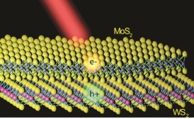 |
| Illustration of a MoS2/WS2 heterostructure with a MoS2 monolayer lying on top of a WS2 monolayer. Electrons and holes created by light are shown to separate into different layers. Image courtesy of Feng Wang group |
Abstract:
A new argument has just been added to the growing case for graphene being bumped off its pedestal as the next big thing in the high-tech world by the two-dimensional semiconductors known as MX2 materials. An international collaboration of researchers led by a scientist with the U.S. Department of Energy (DOE)'s Lawrence Berkeley National Laboratory (Berkeley Lab) has reported the first experimental observation of ultrafast charge transfer in photo-excited MX2 materials. The recorded charge transfer time clocked in at under 50 femtoseconds, comparable to the fastest times recorded for organic photovoltaics.
Competition for Graphene: Berkeley Lab Researchers Demonstrate Ultrafast Charge Transfer in New Family of 2D Semiconductors
Berkeley, CA | Posted on August 26th, 2014"We've demonstrated, for the first time, efficient charge transfer in MX2 heterostructures through combined photoluminescence mapping and transient absorption measurements," says Feng Wang, a condensed matter physicist with Berkeley Lab's Materials Sciences Division and the University of California (UC) Berkeley's Physics Department. "Having quantitatively determined charge transfer time to be less than 50 femtoseconds, our study suggests that MX2 heterostructures, with their remarkable electrical and optical properties and the rapid development of large-area synthesis, hold great promise for future photonic and optoelectronic applications."
Wang is the corresponding author of a paper in Nature Nanotechnology describing this research. The paper is titled "Ultrafast charge transfer in atomically thin MoS2/WS2 heterostructures." Co-authors are Xiaoping Hong, Jonghwan Kim, Su-Fei Shi, Yu Zhang, Chenhao Jin, Yinghui Sun, Sefaattin Tongay, Junqiao Wu and Yanfeng Zhang.
MX2 monolayers consist of a single layer of transition metal atoms, such as molybdenum (Mo) or tungsten (W), sandwiched between two layers of chalcogen atoms, such as sulfur (S). The resulting heterostructure is bound by the relatively weak intermolecular attraction known as the van der Waals force. These 2D semiconductors feature the same hexagonal "honeycombed" structure as graphene and superfast electrical conductance, but, unlike graphene, they have natural energy band-gaps. This facilitates their application in transistors and other electronic devices because, unlike graphene, their electrical conductance can be switched off.
"Combining different MX2 layers together allows one to control their physical properties," says Wang, who is also an investigator with the Kavli Energy NanoSciences Institute (Kavli-ENSI). "For example, the combination of MoS2 and WS2 forms a type-II semiconductor that enables fast charge separation. The separation of photoexcited electrons and holes is essential for driving an electrical current in a photodetector or solar cell."
In demonstrating the ultrafast charge separation capabilities of atomically thin samples of MoS2/WS2 heterostructures, Wang and his collaborators have opened up potentially rich new avenues, not only for photonics and optoelectronics, but also for photovoltaics.
"MX2 semiconductors have extremely strong optical absorption properties and compared with organic photovoltaic materials, have a crystalline structure and better electrical transport properties," Wang says. "Factor in a femtosecond charge transfer rate and MX2 semiconductors provide an ideal way to spatially separate electrons and holes for electrical collection and utilization."
Wang and his colleagues are studying the microscopic origins of charge transfer in MX2 heterostructures and the variation in charge transfer rates between different MX2 materials.
"We're also interested in controlling the charge transfer process with external electrical fields as a means of utilizing MX2 heterostructures in photovoltaic devices," Wang says.
This research was supported by an Early Career Research Award from the DOE Office of Science through UC Berkeley, and by funding agencies in China through the Peking University in Beijing.
####
About DOE/Lawrence Berkeley National Laboratory
Lawrence Berkeley National Laboratory addresses the world�s most urgent scientific challenges by advancing sustainable energy, protecting human health, creating new materials, and revealing the origin and fate of the universe. Founded in 1931, Berkeley Lab�s scientific expertise has been recognized with 13 Nobel prizes. The University of California manages Berkeley Lab for the U.S. Department of Energy�s Office of Science. For more, visit www.lbl.gov.
The DOE Office of Science is the single largest supporter of basic research in the physical sciences in the United States and is working to address some of the most pressing challenges of our time. For more information, please visit science.energy.gov.
- See more at: http://newscenter.lbl.gov/2014/08/26/competition-for-graphene/#sthash.bEFVfG5P.dpuf
For more information, please click here
Contacts:
Lynn Yarris
510-486-5375
Copyright © DOE/Lawrence Berkeley National Laboratory
If you have a comment, please Contact us.Issuers of news releases, not 7th Wave, Inc. or Nanotechnology Now, are solely responsible for the accuracy of the content.
Bookmark:


| Related Links |
![]() For more about the research of Feng Wang go here:
For more about the research of Feng Wang go here:
| Related News Press |
News and information
![]() Quantum computer improves AI predictions April 17th, 2026
Quantum computer improves AI predictions April 17th, 2026
![]() Flexible sensor gains sensitivity under pressure April 17th, 2026
Flexible sensor gains sensitivity under pressure April 17th, 2026
![]() A reusable chip for particulate matter sensing April 17th, 2026
A reusable chip for particulate matter sensing April 17th, 2026
![]() Detecting vibrational quantum beating in the predissociation dynamics of SF6 using time-resolved photoelectron spectroscopy April 17th, 2026
Detecting vibrational quantum beating in the predissociation dynamics of SF6 using time-resolved photoelectron spectroscopy April 17th, 2026
Laboratories
![]() Researchers develop molecular qubits that communicate at telecom frequencies October 3rd, 2025
Researchers develop molecular qubits that communicate at telecom frequencies October 3rd, 2025
Graphene/ Graphite
![]() Electrifying results shed light on graphene foam as a potential material for lab grown cartilage June 6th, 2025
Electrifying results shed light on graphene foam as a potential material for lab grown cartilage June 6th, 2025
![]() Breakthrough in proton barrier films using pore-free graphene oxide: Kumamoto University researchers achieve new milestone in advanced coating technologies September 13th, 2024
Breakthrough in proton barrier films using pore-free graphene oxide: Kumamoto University researchers achieve new milestone in advanced coating technologies September 13th, 2024
Govt.-Legislation/Regulation/Funding/Policy
![]() Quantum computer improves AI predictions April 17th, 2026
Quantum computer improves AI predictions April 17th, 2026
![]() Metasurfaces smooth light to boost magnetic sensing precision January 30th, 2026
Metasurfaces smooth light to boost magnetic sensing precision January 30th, 2026
![]() New imaging approach transforms study of bacterial biofilms August 8th, 2025
New imaging approach transforms study of bacterial biofilms August 8th, 2025
Chip Technology
![]() A reusable chip for particulate matter sensing April 17th, 2026
A reusable chip for particulate matter sensing April 17th, 2026
![]() Metasurfaces smooth light to boost magnetic sensing precision January 30th, 2026
Metasurfaces smooth light to boost magnetic sensing precision January 30th, 2026
Nanoelectronics
![]() Lab to industry: InSe wafer-scale breakthrough for future electronics August 8th, 2025
Lab to industry: InSe wafer-scale breakthrough for future electronics August 8th, 2025
![]() Interdisciplinary: Rice team tackles the future of semiconductors Multiferroics could be the key to ultralow-energy computing October 6th, 2023
Interdisciplinary: Rice team tackles the future of semiconductors Multiferroics could be the key to ultralow-energy computing October 6th, 2023
![]() Key element for a scalable quantum computer: Physicists from Forschungszentrum J�lich and RWTH Aachen University demonstrate electron transport on a quantum chip September 23rd, 2022
Key element for a scalable quantum computer: Physicists from Forschungszentrum J�lich and RWTH Aachen University demonstrate electron transport on a quantum chip September 23rd, 2022
![]() Reduced power consumption in semiconductor devices September 23rd, 2022
Reduced power consumption in semiconductor devices September 23rd, 2022
Discoveries
![]() Quantum computer improves AI predictions April 17th, 2026
Quantum computer improves AI predictions April 17th, 2026
![]() Flexible sensor gains sensitivity under pressure April 17th, 2026
Flexible sensor gains sensitivity under pressure April 17th, 2026
![]() A reusable chip for particulate matter sensing April 17th, 2026
A reusable chip for particulate matter sensing April 17th, 2026
![]() Detecting vibrational quantum beating in the predissociation dynamics of SF6 using time-resolved photoelectron spectroscopy April 17th, 2026
Detecting vibrational quantum beating in the predissociation dynamics of SF6 using time-resolved photoelectron spectroscopy April 17th, 2026
Materials/Metamaterials/Magnetoresistance
![]() First real-time observation of two-dimensional melting process: Researchers at Mainz University unveil new insights into magnetic vortex structures August 8th, 2025
First real-time observation of two-dimensional melting process: Researchers at Mainz University unveil new insights into magnetic vortex structures August 8th, 2025
![]() Researchers unveil a groundbreaking clay-based solution to capture carbon dioxide and combat climate change June 6th, 2025
Researchers unveil a groundbreaking clay-based solution to capture carbon dioxide and combat climate change June 6th, 2025
![]() A 1960s idea inspires NBI researchers to study hitherto inaccessible quantum states June 6th, 2025
A 1960s idea inspires NBI researchers to study hitherto inaccessible quantum states June 6th, 2025
![]() Institute for Nanoscience hosts annual proposal planning meeting May 16th, 2025
Institute for Nanoscience hosts annual proposal planning meeting May 16th, 2025
Announcements
![]() A fundamentally new therapeutic approach to cystic fibrosis: Nanobody repairs cellular defect April 17th, 2026
A fundamentally new therapeutic approach to cystic fibrosis: Nanobody repairs cellular defect April 17th, 2026
![]() UC Irvine physicists discover method to reverse �quantum scrambling� : The work addresses the problem of information loss in quantum computing system April 17th, 2026
UC Irvine physicists discover method to reverse �quantum scrambling� : The work addresses the problem of information loss in quantum computing system April 17th, 2026
Interviews/Book Reviews/Essays/Reports/Podcasts/Journals/White papers/Posters
![]() A fundamentally new therapeutic approach to cystic fibrosis: Nanobody repairs cellular defect April 17th, 2026
A fundamentally new therapeutic approach to cystic fibrosis: Nanobody repairs cellular defect April 17th, 2026
![]() UC Irvine physicists discover method to reverse �quantum scrambling� : The work addresses the problem of information loss in quantum computing system April 17th, 2026
UC Irvine physicists discover method to reverse �quantum scrambling� : The work addresses the problem of information loss in quantum computing system April 17th, 2026
Energy
![]() Sensors innovations for smart lithium-based batteries: advancements, opportunities, and potential challenges August 8th, 2025
Sensors innovations for smart lithium-based batteries: advancements, opportunities, and potential challenges August 8th, 2025
![]() Simple algorithm paired with standard imaging tool could predict failure in lithium metal batteries August 8th, 2025
Simple algorithm paired with standard imaging tool could predict failure in lithium metal batteries August 8th, 2025
Photonics/Optics/Lasers
![]() Metasurfaces smooth light to boost magnetic sensing precision January 30th, 2026
Metasurfaces smooth light to boost magnetic sensing precision January 30th, 2026
![]() From sensors to smart systems: the rise of AI-driven photonic noses January 30th, 2026
From sensors to smart systems: the rise of AI-driven photonic noses January 30th, 2026
Research partnerships
![]() Lab to industry: InSe wafer-scale breakthrough for future electronics August 8th, 2025
Lab to industry: InSe wafer-scale breakthrough for future electronics August 8th, 2025
![]() HKU physicists uncover hidden order in the quantum world through deconfined quantum critical points April 25th, 2025
HKU physicists uncover hidden order in the quantum world through deconfined quantum critical points April 25th, 2025
Solar/Photovoltaic
![]() Spinel-type sulfide semiconductors to operate the next-generation LEDs and solar cells For solar-cell absorbers and green-LED source October 3rd, 2025
Spinel-type sulfide semiconductors to operate the next-generation LEDs and solar cells For solar-cell absorbers and green-LED source October 3rd, 2025
![]() KAIST researchers introduce new and improved, next-generation perovskite solar cell November 8th, 2024
KAIST researchers introduce new and improved, next-generation perovskite solar cell November 8th, 2024
![]() Groundbreaking precision in single-molecule optoelectronics August 16th, 2024
Groundbreaking precision in single-molecule optoelectronics August 16th, 2024
![]() Development of zinc oxide nanopagoda array photoelectrode: photoelectrochemical water-splitting hydrogen production January 12th, 2024
Development of zinc oxide nanopagoda array photoelectrode: photoelectrochemical water-splitting hydrogen production January 12th, 2024
|
|
||
|
|
||
| The latest news from around the world, FREE | ||
|
|
||
|
|
||
| Premium Products | ||
|
|
||
|
Only the news you want to read!
Learn More |
||
|
|
||
|
Full-service, expert consulting
Learn More |
||
|
|
||