Home > Press > Cameca launches next generation atom probe microscope: New LEAP® 5000 Delivers Unmatched 3D Sub-Nanometer Analytical Performance across a Wide Variety of Metals, Semiconductors and Insulators
 |
Abstract:
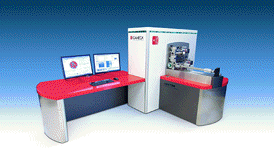
CAMECA, a world leader in scientific instrumentation and metrology solutions, is pleased to announce the release of its latest generation atom probe microscope. The LEAP 5000 offers unparalleled 3-dimensional nano-scale surface, bulk and interfacial materials analysis with atom-by-atom identification and accurate spatial positioning.
Cameca launches next generation atom probe microscope: New LEAP® 5000 Delivers Unmatched 3D Sub-Nanometer Analytical Performance across a Wide Variety of Metals, Semiconductors and Insulators
Madison, WI | Posted on August 6th, 2014"CAMECA is very proud to introduce the LEAP 5000," notes Dr. Tom Kelly, CAMECA Vice President for Innovation and New Technologies, and inventor of the Local Electrode™ Atom Probe (LEAP) technique. "This highly sophisticated materials analysis instrument integrates mature technologies from previous LEAP models and comes equipped with a redesigned detection system offering increased efficiency, advanced laser control, faster data collection and real-time monitoring capabilities, all housed in a more robust and ergonomic platform."
Thanks to these advances along with greatly enhanced ease-of-use and productivity, the LEAP 5000 continues to set the industry standard in providing the ultimate in analytical accuracy, sensitivity, and 3D spatial resolution across a wide variety of metals, semiconductors and insulators. Most importantly, the LEAP 5000 will assist scientists and engineers around the world in accelerating discoveries and developing novel materials, products and devices.
Atom Probe Tomography (APT or 3D APT) is the only materials analysis technique offering extensive capability for both 3D imaging and chemical composition measurements at the atomic scale. Since its development in the 1960s, the technique has contributed to major advances in materials science.
Exclusively developed and manufactured by CAMECA, LEAP microscopes are used by the most prestigious research and development laboratories around the world, including seven of the ten largest computer chip manufacturers.
####
About CAMECA
CAMECA® has more than 60 years of experience in the design, manufacture and servicing of scientific instruments for material micro- and nano-analysis. Since pioneering Electron Probe Microanalysis (EPMA) instrumentation in the 1950s and Secondary Ion Mass Spectrometry (SIMS) in the 1960s, CAMECA has remained the undisputed world leader, while achieving numerous breakthrough innovations in such complementary techniques as Low-energy Electron-induced X-ray Emission Spectrometry (LEXES) and Atom Probe Tomography (APT).
Headquartered near Paris, CAMECA also has a production facility in Madison WI, USA (where the LEAP APT is designed and manufactured), and further locations in Brazil, China, England, Germany, India, Japan, Korea, and Taiwan. CAMECA is a business unit of the Materials Analysis Division of AMETEK® Inc., a leading global manufacturer of electronic instruments and electromechanical products.
For more information, please click here
Contacts:
Curt Scheppmann
Phone: + 1 608 229 1933
Copyright © CAMECA
If you have a comment, please Contact us.Issuers of news releases, not 7th Wave, Inc. or Nanotechnology Now, are solely responsible for the accuracy of the content.
Bookmark:


| Related News Press |
News and information
![]() Quantum computer improves AI predictions April 17th, 2026
Quantum computer improves AI predictions April 17th, 2026
![]() Flexible sensor gains sensitivity under pressure April 17th, 2026
Flexible sensor gains sensitivity under pressure April 17th, 2026
![]() A reusable chip for particulate matter sensing April 17th, 2026
A reusable chip for particulate matter sensing April 17th, 2026
![]() Detecting vibrational quantum beating in the predissociation dynamics of SF6 using time-resolved photoelectron spectroscopy April 17th, 2026
Detecting vibrational quantum beating in the predissociation dynamics of SF6 using time-resolved photoelectron spectroscopy April 17th, 2026
Imaging
![]() Simple algorithm paired with standard imaging tool could predict failure in lithium metal batteries August 8th, 2025
Simple algorithm paired with standard imaging tool could predict failure in lithium metal batteries August 8th, 2025
Chip Technology
![]() A reusable chip for particulate matter sensing April 17th, 2026
A reusable chip for particulate matter sensing April 17th, 2026
![]() Metasurfaces smooth light to boost magnetic sensing precision January 30th, 2026
Metasurfaces smooth light to boost magnetic sensing precision January 30th, 2026
Announcements
![]() A fundamentally new therapeutic approach to cystic fibrosis: Nanobody repairs cellular defect April 17th, 2026
A fundamentally new therapeutic approach to cystic fibrosis: Nanobody repairs cellular defect April 17th, 2026
![]() UC Irvine physicists discover method to reverse ‘quantum scrambling’ : The work addresses the problem of information loss in quantum computing system April 17th, 2026
UC Irvine physicists discover method to reverse ‘quantum scrambling’ : The work addresses the problem of information loss in quantum computing system April 17th, 2026
Tools
![]() Metasurfaces smooth light to boost magnetic sensing precision January 30th, 2026
Metasurfaces smooth light to boost magnetic sensing precision January 30th, 2026
![]() From sensors to smart systems: the rise of AI-driven photonic noses January 30th, 2026
From sensors to smart systems: the rise of AI-driven photonic noses January 30th, 2026
![]() Japan launches fully domestically produced quantum computer: Expo visitors to experience quantum computing firsthand August 8th, 2025
Japan launches fully domestically produced quantum computer: Expo visitors to experience quantum computing firsthand August 8th, 2025
|
|
||
|
|
||
| The latest news from around the world, FREE | ||
|
|
||
|
|
||
| Premium Products | ||
|
|
||
|
Only the news you want to read!
Learn More |
||
|
|
||
|
Full-service, expert consulting
Learn More |
||
|
|
||