Home > Press > NUS scientists use low cost technique to improve properties and functions of nanomaterials: By 'drawing' micropatterns on nanomaterials using a focused laser beam, scientists could modify properties of nanomaterials for effective applications in photonic and optoelectric applicat
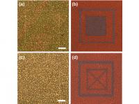 |
| Mesoporous silicon nanowires were scanned by a focused laser beam in two different patterns, imaged by bright-field optical microscope, as depicted by (a) and (c), as well as fluorescence microscopy, as depicted by (b) and (d). Evidently, the images hidden in boxes shown in (a) and (c) are clearly revealed under fluorescence microscopy.
Credit: National University of Singapore |
Abstract:
The challenges faced by researchers in modifying properties of nanomaterials for application in devices may be addressed by a simple technique, thanks to recent innovative studies conducted by scientists from the National University of Singapore (NUS).
NUS scientists use low cost technique to improve properties and functions of nanomaterials: By 'drawing' micropatterns on nanomaterials using a focused laser beam, scientists could modify properties of nanomaterials for effective applications in photonic and optoelectric applicat
Singapore | Posted on July 22nd, 2014Through the use of a simple, efficient and low cost technique involving a focused laser beam, two NUS research teams, led by Professor Sow Chorng Haur from the Department of Physics at the NUS Faculty of Science, demonstrated that the properties of two different types of materials can be controlled and modified, and consequently, their functionalities can be enhanced.
Said Prof Sow, "In our childhood, most of us are likely to have the experience of bringing a magnifying glass outdoors on a sunny day and tried to focus sunlight onto a piece of paper to burn the paper. Such a simple approach turns out to be a very versatile tool in research. Instead of focusing sunlight, we can focus laser beam onto a wide variety of nanomaterials and study effects of the focused laser beam has on these materials."
Micropatterns 'drawn' on MoS2 films could enhance electrical conductivity and photoconductivity
Molybdenum disulfide (MoS2), a class of transition metal dichalcogenide compound, has attracted great attention as an emerging two-dimensional (2D) material due to wide recognition of its potential in and optoelectronics. One of the many fascinating properties of 2D MoS2 film is that its properties depend on the thickness of the film. In addition, its properties can be modified once the film is modified chemically. Hence one of the challenges in this field is the ability to create microdevices out of the MoS2 film comprising components with different thickness or chemical nature.
To address this technological challenge, Prof Sow, Dr Lu Junpeng, a postdoctoral candidate from the Department of Physics at the NUS Faculty of Science, as well as their team members, utilised an optical microscope-focused laser beam setup to 'draw' micropatterns directly onto large area MoS2 films as well as to thin the films.
With this simple and low cost approach, the scientists were able to use the focused laser beam to selectively 'draw' patterns onto any region of the film to modify properties of the desired area, unlike other current methods where the entire film is modified.
Interestingly, they also found that the electrical conductivity and photoconductivity of the modified material had increased by more than 10 times and about five times respectively. The research team fabricated a photodetector using laser modified MoS2 film and demonstrated the superior performance of MoS2 for such application.
This innovation was first published online in the journal ACS Nano on 24 May 2014.
Hidden images 'drawn' by focused laser beam on silicon nanowires could improve optical functionalities
In a related study published in the journal Scientific Reports on 13 May 2014, Prof Sow led another team of researchers from the NUS Faculty of Science, in collaboration with scientists from Hong Kong Baptist University, to investigate how 'drawing' micropatterns on mesoporous silicon nanowires could change the properties of nanowires and advance their applications.
The team scanned a focused laser beam rapidly onto an array of mesoporous silicon nanowires, which are closely packed like the tightly woven threads of a carpet. They found that the focused laser beam could modify the optical properties of the nanowires, causing them to emit greenish-blue fluorescence light. This is the first observation of such a laser-modified behaviour from the mesoporous silicon nanowires to be reported.
The researchers systematically studied the laser-induced modification to gain insights into establishing control over the optical properties of the mesoporous silicon nanowires. Their understanding enabled them to 'draw' a wide variety of micropatterns with different optical functionalities using the focused laser beam.
To put their findings to the test, the researchers engineered the functional components of the nanowires with interesting applications. The research team demonstrated that the micropatterns created at a low laser power are invisible under bright-field optical microscope, but become apparent under fluorescence microscope, indicating the feasibility of hidden images.
Further research
The fast growing field of electronics and optoelectronics demands precise material deposition with application-specific optical, electrical, chemical, and mechanical properties.
To develop materials with properties that can cater to the industry's demands, Prof Sow, together with his team of researchers, will extend the versatile focused laser beam technique to more nanomaterials. In addition, they will look into further improving the properties of MoS2 and mesoporous silicon with different techniques.
####
For more information, please click here
Contacts:
Carolyn Fong
65-651-65399
Copyright © National University of Singapore
If you have a comment, please Contact us.Issuers of news releases, not 7th Wave, Inc. or Nanotechnology Now, are solely responsible for the accuracy of the content.
Bookmark:


| Related News Press |
News and information
![]() Quantum computer improves AI predictions April 17th, 2026
Quantum computer improves AI predictions April 17th, 2026
![]() Flexible sensor gains sensitivity under pressure April 17th, 2026
Flexible sensor gains sensitivity under pressure April 17th, 2026
![]() A reusable chip for particulate matter sensing April 17th, 2026
A reusable chip for particulate matter sensing April 17th, 2026
![]() Detecting vibrational quantum beating in the predissociation dynamics of SF6 using time-resolved photoelectron spectroscopy April 17th, 2026
Detecting vibrational quantum beating in the predissociation dynamics of SF6 using time-resolved photoelectron spectroscopy April 17th, 2026
Chip Technology
![]() A reusable chip for particulate matter sensing April 17th, 2026
A reusable chip for particulate matter sensing April 17th, 2026
![]() Metasurfaces smooth light to boost magnetic sensing precision January 30th, 2026
Metasurfaces smooth light to boost magnetic sensing precision January 30th, 2026
Optical computing/Photonic computing
![]() ICFO researchers overcome long-standing bottleneck in single photon detection with twisted 2D materials August 8th, 2025
ICFO researchers overcome long-standing bottleneck in single photon detection with twisted 2D materials August 8th, 2025
![]() Programmable electron-induced color router array May 14th, 2025
Programmable electron-induced color router array May 14th, 2025
Discoveries
![]() Quantum computer improves AI predictions April 17th, 2026
Quantum computer improves AI predictions April 17th, 2026
![]() Flexible sensor gains sensitivity under pressure April 17th, 2026
Flexible sensor gains sensitivity under pressure April 17th, 2026
![]() A reusable chip for particulate matter sensing April 17th, 2026
A reusable chip for particulate matter sensing April 17th, 2026
![]() Detecting vibrational quantum beating in the predissociation dynamics of SF6 using time-resolved photoelectron spectroscopy April 17th, 2026
Detecting vibrational quantum beating in the predissociation dynamics of SF6 using time-resolved photoelectron spectroscopy April 17th, 2026
Materials/Metamaterials/Magnetoresistance
![]() First real-time observation of two-dimensional melting process: Researchers at Mainz University unveil new insights into magnetic vortex structures August 8th, 2025
First real-time observation of two-dimensional melting process: Researchers at Mainz University unveil new insights into magnetic vortex structures August 8th, 2025
![]() Researchers unveil a groundbreaking clay-based solution to capture carbon dioxide and combat climate change June 6th, 2025
Researchers unveil a groundbreaking clay-based solution to capture carbon dioxide and combat climate change June 6th, 2025
![]() A 1960s idea inspires NBI researchers to study hitherto inaccessible quantum states June 6th, 2025
A 1960s idea inspires NBI researchers to study hitherto inaccessible quantum states June 6th, 2025
![]() Institute for Nanoscience hosts annual proposal planning meeting May 16th, 2025
Institute for Nanoscience hosts annual proposal planning meeting May 16th, 2025
Announcements
![]() A fundamentally new therapeutic approach to cystic fibrosis: Nanobody repairs cellular defect April 17th, 2026
A fundamentally new therapeutic approach to cystic fibrosis: Nanobody repairs cellular defect April 17th, 2026
![]() UC Irvine physicists discover method to reverse �quantum scrambling� : The work addresses the problem of information loss in quantum computing system April 17th, 2026
UC Irvine physicists discover method to reverse �quantum scrambling� : The work addresses the problem of information loss in quantum computing system April 17th, 2026
Interviews/Book Reviews/Essays/Reports/Podcasts/Journals/White papers/Posters
![]() A fundamentally new therapeutic approach to cystic fibrosis: Nanobody repairs cellular defect April 17th, 2026
A fundamentally new therapeutic approach to cystic fibrosis: Nanobody repairs cellular defect April 17th, 2026
![]() UC Irvine physicists discover method to reverse �quantum scrambling� : The work addresses the problem of information loss in quantum computing system April 17th, 2026
UC Irvine physicists discover method to reverse �quantum scrambling� : The work addresses the problem of information loss in quantum computing system April 17th, 2026
Photonics/Optics/Lasers
![]() Metasurfaces smooth light to boost magnetic sensing precision January 30th, 2026
Metasurfaces smooth light to boost magnetic sensing precision January 30th, 2026
![]() From sensors to smart systems: the rise of AI-driven photonic noses January 30th, 2026
From sensors to smart systems: the rise of AI-driven photonic noses January 30th, 2026
|
|
||
|
|
||
| The latest news from around the world, FREE | ||
|
|
||
|
|
||
| Premium Products | ||
|
|
||
|
Only the news you want to read!
Learn More |
||
|
|
||
|
Full-service, expert consulting
Learn More |
||
|
|
||