Home > Press > With 'ribbons' of graphene, width matters: A narrow enough ribbon will transform a high-performance conductor into a semiconductor
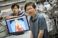 |
| Yaoyi Li (foreground) and Mingxing Chen, UWM physics postdoctoral researchers, display an image of a ribbon of graphene 1 nanometer wide. In the image, achieved with a scanning-tunneling microscope, atoms are visible as "bumps."
Credit: Troye Fox, UWM Photo Services |
Abstract:
Using graphene ribbons of unimaginably small widths - just several atoms across - a group of researchers at the University of Wisconsin-Milwaukee (UWM) has found a novel way to "tune" the wonder material, causing the extremely efficient conductor of electricity to act as a semiconductor.
With 'ribbons' of graphene, width matters: A narrow enough ribbon will transform a high-performance conductor into a semiconductor
Milwaukee, WI | Posted on July 4th, 2014In principle, their method for producing these narrow ribbons - at a width roughly equal to the diameter of a strand of human DNA - and manipulating the ribbons' electrical conductivity could be used to produce nano-devices.
Graphene, a one-atom-thick sheet of carbon atoms, is touted for its high potential to yield devices at nanoscale and deliver computing at quantum speed. But before it can be applied to nanotechnology, researchers must first find an easy method of controlling the flow of electrons in order to devise even a simple on-off switch.
"Nano-ribbons are model systems for studying nanoscale effects in graphene, but obtaining a ribbon width below 10 nanometers and characterizing its electronic state is quite challenging," says Yaoyi Li, a UWM physics postdoctoral researcher and first author of a paper published July 2 in the journal Nature Communications.
By imaging the ribbons with scanning-tunneling microscopy, researchers have confirmed how narrow the ribbon width must be to alter graphene's electrical properties, making it more tunable.
"We found the transition happens at three nanometers and the changes are abrupt," says Michael Weinert, a UWM theoretical physicist who worked on the Department of Energy-supported project with experimental physicist Lian Li. "Before this study, there was no experimental evidence of what width the onset of these behaviors is."
The team also found that the narrower the ribbon becomes, the more "tunable" the material's behaviors. The two edges of such a narrow ribbon are able to strongly interact, essentially transforming the ribbon into a semiconductor with tunable qualities similar to that of silicon.
The first hurdle
Current methods of cutting can produce ribbon widths of five nanometers across, still too wide to achieve the tunable state, says Yaoyi Li. In addition to producing narrower ribbons, any new strategy for cutting they devised would also have to result in a straight alignment of the atoms at the ribbon edges in order to maintain the electrical properties, he adds.
So the UWM team used iron nanoparticles on top of the graphene in a hydrogen environment. Iron is a catalyst that causes hydrogen and carbon atoms to react, creating a gas that etches a trench into the graphene. The cutting is accomplished by precisely controlling the hydrogen pressure, says Lian Li.
The iron nanoparticle moves randomly across the graphene, producing ribbons of various widths - including some as thin as one nanometer, he says. The method also produces edges with properly aligned atoms.
One limitation exists for the team's cutting method, and that has to do with where the edges are cut. The atoms in graphene are arranged on a honeycomb lattice that, depending on the direction of the cut produces either an "armchair-shaped" edge or a "zigzag" one. The semiconducting behaviors the researchers observed with their etching method will only occur with a cut in the zigzag configuration.
Manipulating for function
When cut, the carbon atoms at the edges of the resulting ribbons have only two of the normal three neighbors, creating a kind of bond that attracts hydrogen atoms and corrals electrons to the edges of the ribbon. If the ribbon is narrow enough, the electrons on opposite sides can still interact, creating a semiconductive electrical behavior, says Weinert.
The researchers are now experimenting with saturating the edges with oxygen, rather than hydrogen, to investigate whether this changes the electrical behavior of the graphene to that of a metal.
Adding function to graphene nano-ribbons through this process could make possible the sought-after goal of atomic-scale components made of the same material, but with different electrical behaviors, says Weinert.
####
For more information, please click here
Contacts:
Lian Li
414-229-5108
Copyright © University of Wisconsin - Milwaukee
If you have a comment, please Contact us.Issuers of news releases, not 7th Wave, Inc. or Nanotechnology Now, are solely responsible for the accuracy of the content.
Bookmark:


| Related News Press |
News and information
![]() Quantum computer improves AI predictions April 17th, 2026
Quantum computer improves AI predictions April 17th, 2026
![]() Flexible sensor gains sensitivity under pressure April 17th, 2026
Flexible sensor gains sensitivity under pressure April 17th, 2026
![]() A reusable chip for particulate matter sensing April 17th, 2026
A reusable chip for particulate matter sensing April 17th, 2026
![]() Detecting vibrational quantum beating in the predissociation dynamics of SF6 using time-resolved photoelectron spectroscopy April 17th, 2026
Detecting vibrational quantum beating in the predissociation dynamics of SF6 using time-resolved photoelectron spectroscopy April 17th, 2026
Graphene/ Graphite
![]() Electrifying results shed light on graphene foam as a potential material for lab grown cartilage June 6th, 2025
Electrifying results shed light on graphene foam as a potential material for lab grown cartilage June 6th, 2025
![]() Breakthrough in proton barrier films using pore-free graphene oxide: Kumamoto University researchers achieve new milestone in advanced coating technologies September 13th, 2024
Breakthrough in proton barrier films using pore-free graphene oxide: Kumamoto University researchers achieve new milestone in advanced coating technologies September 13th, 2024
Molecular Nanotechnology
![]() Quantum pumping in molecular junctions August 16th, 2024
Quantum pumping in molecular junctions August 16th, 2024
![]() Scientists push the boundaries of manipulating light at the submicroscopic level March 3rd, 2023
Scientists push the boundaries of manipulating light at the submicroscopic level March 3rd, 2023
![]() First electric nanomotor made from DNA material: Synthetic rotary motors at the nanoscale perform mechanical work July 22nd, 2022
First electric nanomotor made from DNA material: Synthetic rotary motors at the nanoscale perform mechanical work July 22nd, 2022
Chip Technology
![]() A reusable chip for particulate matter sensing April 17th, 2026
A reusable chip for particulate matter sensing April 17th, 2026
![]() Metasurfaces smooth light to boost magnetic sensing precision January 30th, 2026
Metasurfaces smooth light to boost magnetic sensing precision January 30th, 2026
Nanoelectronics
![]() Lab to industry: InSe wafer-scale breakthrough for future electronics August 8th, 2025
Lab to industry: InSe wafer-scale breakthrough for future electronics August 8th, 2025
![]() Interdisciplinary: Rice team tackles the future of semiconductors Multiferroics could be the key to ultralow-energy computing October 6th, 2023
Interdisciplinary: Rice team tackles the future of semiconductors Multiferroics could be the key to ultralow-energy computing October 6th, 2023
![]() Key element for a scalable quantum computer: Physicists from Forschungszentrum J�lich and RWTH Aachen University demonstrate electron transport on a quantum chip September 23rd, 2022
Key element for a scalable quantum computer: Physicists from Forschungszentrum J�lich and RWTH Aachen University demonstrate electron transport on a quantum chip September 23rd, 2022
![]() Reduced power consumption in semiconductor devices September 23rd, 2022
Reduced power consumption in semiconductor devices September 23rd, 2022
Discoveries
![]() Quantum computer improves AI predictions April 17th, 2026
Quantum computer improves AI predictions April 17th, 2026
![]() Flexible sensor gains sensitivity under pressure April 17th, 2026
Flexible sensor gains sensitivity under pressure April 17th, 2026
![]() A reusable chip for particulate matter sensing April 17th, 2026
A reusable chip for particulate matter sensing April 17th, 2026
![]() Detecting vibrational quantum beating in the predissociation dynamics of SF6 using time-resolved photoelectron spectroscopy April 17th, 2026
Detecting vibrational quantum beating in the predissociation dynamics of SF6 using time-resolved photoelectron spectroscopy April 17th, 2026
Announcements
![]() A fundamentally new therapeutic approach to cystic fibrosis: Nanobody repairs cellular defect April 17th, 2026
A fundamentally new therapeutic approach to cystic fibrosis: Nanobody repairs cellular defect April 17th, 2026
![]() UC Irvine physicists discover method to reverse �quantum scrambling� : The work addresses the problem of information loss in quantum computing system April 17th, 2026
UC Irvine physicists discover method to reverse �quantum scrambling� : The work addresses the problem of information loss in quantum computing system April 17th, 2026
Interviews/Book Reviews/Essays/Reports/Podcasts/Journals/White papers/Posters
![]() A fundamentally new therapeutic approach to cystic fibrosis: Nanobody repairs cellular defect April 17th, 2026
A fundamentally new therapeutic approach to cystic fibrosis: Nanobody repairs cellular defect April 17th, 2026
![]() UC Irvine physicists discover method to reverse �quantum scrambling� : The work addresses the problem of information loss in quantum computing system April 17th, 2026
UC Irvine physicists discover method to reverse �quantum scrambling� : The work addresses the problem of information loss in quantum computing system April 17th, 2026
|
|
||
|
|
||
| The latest news from around the world, FREE | ||
|
|
||
|
|
||
| Premium Products | ||
|
|
||
|
Only the news you want to read!
Learn More |
||
|
|
||
|
Full-service, expert consulting
Learn More |
||
|
|
||