Home > Press > New rapid synthesis developed for bilayer graphene and high-performance transistors: UCSB researchers demonstrate ultra-fast and deterministic growth of high-quality and large-area bilayer graphene films with controlled stacking order required for low-power digital electronics
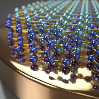 |
| This is concept art of a schematic view of an AB-stacked graphene film synthesized by UC Santa Barbara researchers using a stoichiometry engineered bifunctional alloy catalyst.
Credit: Peter Allen, UCSB |
Abstract:
Researchers at University of California, Santa Barbara, in collaboration with Rice University, have recently demonstrated a rapid synthesis technique for large-area Bernal (or AB) stacked bilayer graphene films that can open up new pathways for digital electronics and transparent conductor applications.
New rapid synthesis developed for bilayer graphene and high-performance transistors: UCSB researchers demonstrate ultra-fast and deterministic growth of high-quality and large-area bilayer graphene films with controlled stacking order required for low-power digital electronics
Santa Barbara, CA | Posted on May 3rd, 2014The invention also includes the first demonstration of a bilayer graphene double-gate field-effect transistor (FET), showing record ON/OFF transistor switching ratio and carrier mobility that could drive future ultra-low power and low-cost electronics.
Graphene is the thinnest known (~0.5 nanometer per layer) 2-dimensional atomic crystal. It has attracted wide interest due to its promising electrical and thermal properties and potential applications in electronics and photonics. However, many of those applications are significantly restricted by the zero band gap of graphene that results in leaky transistors not suitable for digital electronics.
"In addition to its atomically smooth surfaces, a considerable band gap of up to ~0.25 eV can be opened up in bilayer graphene by creating a potential difference between the two layers, and thereby breaking the inherent symmetry, if the two layers can be aligned along a certain (Bernal or AB) orientation" explained Kaustav Banerjee, professor of electrical and computer engineering and Director of the Nanoelectronics Research Lab at UCSB. "The dual-gated transistors were specifically designed to allow such potential difference to be established between the layers through one of the gates, while the second gate modulated the carriers in the channel," he added. Banerjee's research team also includes UCSB researchers Wei Liu, Stephan Kraemer, Deblina Sarkar, Hong Li and Professor Pulickel Ajayan of Rice University. Their study was recently published in Chemistry of Materials.
The graphene films were grown in a deterministic manner using an engineered bifunctional (Cu:Ni) alloy surface at a relatively low temperature of 920 �C. Large-area (> 3 inch � 3 inch) Bernal (or AB) stacked bilayer graphene growth was demonstrated within few minutes and with nearly 100% area coverage. The bilayer graphene films exhibited electron mobility as high as 3450 cm2/(V�s), which is comparable to that of exfoliated bilayer graphene, thereby confirming very high-quality. The quality of grown graphene was further corroborated by demonstration of high-performance FETs with record ON/OFF ratio that is a key requirement in low-power digital electronics.
"Achieving surface catalytic graphene growth mode and precise control of the surface carbon concentration were key factors for the favorable growth kinetics for AB stacked bilayer graphene," explained Wei Liu, a post-doctoral researcher in Banerjee's group and a co-author of the article. In 2011, Banerjee's group demonstrated a large-area monolayer graphene synthesis method using a copper substrate as catalyst.
Bilayer graphene is close to monolayer graphene in terms of the film thickness with a hexagonal atomic structure and can be derived from its layered bulk form (graphite) in which adjacent layers are held together by relatively weak van der Waals forces. "However, apart from its band gap tunability, bilayer graphene has some key advantages over monolayer graphene. It has higher density of states and suffers much less from interface effects, which are beneficial for improving the current carrying capability," Liu continued.
"This demonstration is very impressive and should have far-reaching implications for the entire 2D materials community," commented Professor Ali Javey, of University of California, Berkeley and a Co-Director of the Bay Area Photovoltaic Consortium (BAPVC).
###
Their research was supported by the Bay Area Photovoltaic Consortium (BAPVC) a U.S. Department of Energy funded Photovoltaic Consortium, the California NanoSystems Institute at UC Santa Barbara, and the Materials Research Laboratory at UCSB: a National Science Foundation MRSEC.
####
About University of California - Santa Barbara
The College of Engineering at University of California, Santa Barbara is recognized globally as a leader among the top tier of engineering education and research programs, and is renowned for a successful interdisciplinary approach to engineering research. www.engineering.ucsb.edu
For more information, please click here
Contacts:
Melissa Van De Werfhorst
Copyright © University of California - Santa Barbara
If you have a comment, please Contact us.Issuers of news releases, not 7th Wave, Inc. or Nanotechnology Now, are solely responsible for the accuracy of the content.
Bookmark:


| Related News Press |
News and information
![]() Quantum computer improves AI predictions April 17th, 2026
Quantum computer improves AI predictions April 17th, 2026
![]() Flexible sensor gains sensitivity under pressure April 17th, 2026
Flexible sensor gains sensitivity under pressure April 17th, 2026
![]() A reusable chip for particulate matter sensing April 17th, 2026
A reusable chip for particulate matter sensing April 17th, 2026
![]() Detecting vibrational quantum beating in the predissociation dynamics of SF6 using time-resolved photoelectron spectroscopy April 17th, 2026
Detecting vibrational quantum beating in the predissociation dynamics of SF6 using time-resolved photoelectron spectroscopy April 17th, 2026
Graphene/ Graphite
![]() Electrifying results shed light on graphene foam as a potential material for lab grown cartilage June 6th, 2025
Electrifying results shed light on graphene foam as a potential material for lab grown cartilage June 6th, 2025
![]() Breakthrough in proton barrier films using pore-free graphene oxide: Kumamoto University researchers achieve new milestone in advanced coating technologies September 13th, 2024
Breakthrough in proton barrier films using pore-free graphene oxide: Kumamoto University researchers achieve new milestone in advanced coating technologies September 13th, 2024
Govt.-Legislation/Regulation/Funding/Policy
![]() Quantum computer improves AI predictions April 17th, 2026
Quantum computer improves AI predictions April 17th, 2026
![]() Metasurfaces smooth light to boost magnetic sensing precision January 30th, 2026
Metasurfaces smooth light to boost magnetic sensing precision January 30th, 2026
![]() New imaging approach transforms study of bacterial biofilms August 8th, 2025
New imaging approach transforms study of bacterial biofilms August 8th, 2025
Chip Technology
![]() A reusable chip for particulate matter sensing April 17th, 2026
A reusable chip for particulate matter sensing April 17th, 2026
![]() Metasurfaces smooth light to boost magnetic sensing precision January 30th, 2026
Metasurfaces smooth light to boost magnetic sensing precision January 30th, 2026
Nanoelectronics
![]() Lab to industry: InSe wafer-scale breakthrough for future electronics August 8th, 2025
Lab to industry: InSe wafer-scale breakthrough for future electronics August 8th, 2025
![]() Interdisciplinary: Rice team tackles the future of semiconductors Multiferroics could be the key to ultralow-energy computing October 6th, 2023
Interdisciplinary: Rice team tackles the future of semiconductors Multiferroics could be the key to ultralow-energy computing October 6th, 2023
![]() Key element for a scalable quantum computer: Physicists from Forschungszentrum J�lich and RWTH Aachen University demonstrate electron transport on a quantum chip September 23rd, 2022
Key element for a scalable quantum computer: Physicists from Forschungszentrum J�lich and RWTH Aachen University demonstrate electron transport on a quantum chip September 23rd, 2022
![]() Reduced power consumption in semiconductor devices September 23rd, 2022
Reduced power consumption in semiconductor devices September 23rd, 2022
Discoveries
![]() Quantum computer improves AI predictions April 17th, 2026
Quantum computer improves AI predictions April 17th, 2026
![]() Flexible sensor gains sensitivity under pressure April 17th, 2026
Flexible sensor gains sensitivity under pressure April 17th, 2026
![]() A reusable chip for particulate matter sensing April 17th, 2026
A reusable chip for particulate matter sensing April 17th, 2026
![]() Detecting vibrational quantum beating in the predissociation dynamics of SF6 using time-resolved photoelectron spectroscopy April 17th, 2026
Detecting vibrational quantum beating in the predissociation dynamics of SF6 using time-resolved photoelectron spectroscopy April 17th, 2026
Announcements
![]() A fundamentally new therapeutic approach to cystic fibrosis: Nanobody repairs cellular defect April 17th, 2026
A fundamentally new therapeutic approach to cystic fibrosis: Nanobody repairs cellular defect April 17th, 2026
![]() UC Irvine physicists discover method to reverse �quantum scrambling� : The work addresses the problem of information loss in quantum computing system April 17th, 2026
UC Irvine physicists discover method to reverse �quantum scrambling� : The work addresses the problem of information loss in quantum computing system April 17th, 2026
Interviews/Book Reviews/Essays/Reports/Podcasts/Journals/White papers/Posters
![]() A fundamentally new therapeutic approach to cystic fibrosis: Nanobody repairs cellular defect April 17th, 2026
A fundamentally new therapeutic approach to cystic fibrosis: Nanobody repairs cellular defect April 17th, 2026
![]() UC Irvine physicists discover method to reverse �quantum scrambling� : The work addresses the problem of information loss in quantum computing system April 17th, 2026
UC Irvine physicists discover method to reverse �quantum scrambling� : The work addresses the problem of information loss in quantum computing system April 17th, 2026
Research partnerships
![]() Lab to industry: InSe wafer-scale breakthrough for future electronics August 8th, 2025
Lab to industry: InSe wafer-scale breakthrough for future electronics August 8th, 2025
![]() HKU physicists uncover hidden order in the quantum world through deconfined quantum critical points April 25th, 2025
HKU physicists uncover hidden order in the quantum world through deconfined quantum critical points April 25th, 2025
|
|
||
|
|
||
| The latest news from around the world, FREE | ||
|
|
||
|
|
||
| Premium Products | ||
|
|
||
|
Only the news you want to read!
Learn More |
||
|
|
||
|
Full-service, expert consulting
Learn More |
||
|
|
||