Home > Press > Edgy Look at 2D Molybdenum Disulfide: Berkeley Lab Researchers Observe 1D Edge States Critical to Nanoelectronic and Photonic Applications
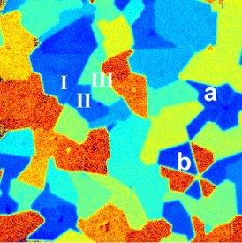 |
| A new SHG imaging technique allows rapid and all-optical determination of the crystal orientations of 2D semiconductor membranes at a large scale, providing the knowledge needed to use these materials in nanoelectronic devices. |
Abstract:
The drive to develop ultrasmall and ultrafast electronic devices using a single atomic layer of semiconductors, such as transition metal dichalcogenides, has received a significant boost. Researchers with the U.S. Department of Energy (DOE)'s Lawrence Berkeley National Laboratory (Berkeley Lab) have recorded the first observations of a strong nonlinear optical resonance along the edges of a single layer of molybdenum disulfide. The existence of these edge states is key to the use of molybdenum disulfide in nanoelectronics, as well as a catalyst for the hydrogen evolution reaction in fuel cells, desulfurization and other chemical reactions.
Edgy Look at 2D Molybdenum Disulfide: Berkeley Lab Researchers Observe 1D Edge States Critical to Nanoelectronic and Photonic Applications
Berkeley, CA | Posted on May 2nd, 2014"We observed strong nonlinear optical resonances at the edges of a two-dimensional crystal of molybdenum disulfide" says Xiang Zhang, a faculty scientist with Berkeley Lab's Materials Sciences Division who led this study. "These one-dimensional edge states are the result of electronic structure changes and may enable novel nanoelectronics and photonic devices. These edges have also long been suspected to be the active sites for the electrocatalytic hydrogen evolution reaction in energy applications. We also discovered extraordinary second harmonic light generation properties that may be used for the in situ monitoring of electronic changes and chemical reactions that occur at the one-dimensional atomic edges."
Zhang, who also holds the Ernest S. Kuh Endowed Chair Professor at the University of California (UC) Berkeley, directs the National Science Foundation's Nano-scale Science and Engineering Center, and is a member of the Kavli Energy NanoSciences Institute at Berkeley, is the corresponding author of a paper in Science describing this research. The paper is titled "Edge Nonlinear Optics on a MoS2 Atomic Monolayer." Co-authors are Xiaobo Yin, Ziliang Ye, Daniel Chenet, Yu Ye, Kevin O'Brien and James Hone.
Emerging two-dimensional semiconductors are prized in the electronics industry for their superior energy efficiency and capacity to carry much higher current densities than silicon. Only a single molecule thick, they are well-suited for integrated optoelectronic devices. Until recently, graphene has been the unchallenged superstar of 2D materials, but today there is considerable attention focused on 2D semiconducting crystals that consist of a single layer of transition metal atoms, such as molybdenum, tungsten or niobium, sandwiched between two layers of chalcogen atoms, such as sulfur or selenium. Featuring the same flat hexagonal "honeycombed" structure as graphene and many of the same electrical advantages, these transition metal dichalcogenides, unlike graphene, have direct energy bandgaps. This facilitates their application in transistors and other electronic devices, particularly light-emitting diodes.
Full realization of the vast potential of transition metal dichalcogenides will only come with a better understanding of the domain orientations of their crystal structures that give rise to their exceptional properties. Until now, however, experimental imaging of these three-atom-thick structures and their edges have been limited to scanning tunneling microscopy and transmission electron microscopy, technologies that are often difficult to use. Nonlinear optics at the crystal edges and boundaries enabled Zhang and his collaborators to develop a new imaging technique based on second-harmonic generation (SHG) light emissions that can easily capture the crystal structures and grain orientations with an optical microscope.
"Our nonlinear optical imaging technique is a non-invasive, fast, easy metrologic approach to the study of 2D atomic materials," says Xiaobo Yin, the lead author of the Science paper and a former member of Zhang's research group who is now on the faculty at the University of Colorado, Boulder. "We don't need to prepare the sample on any special substrate or vacuum environment, and the measurement won't perturb the sample during the imaging process. This advantage allows for in-situ measurements under many practical conditions. Furthermore, our imaging technique is an ultrafast measurement that can provide critical dynamic information, and its instrumentation is far less complicated and less expensive compared with scanning tunneling microscopy and transmission electron microscopy."
For the SHG imaging of molybdenum disulfide, Zhang and his collaborators illuminated sample membranes that are only three atoms thick with ultrafast pulses of infrared light. The nonlinear optical properties of the samples yielded a strong SHG response in the form of visible light that is both tunable and coherent. The resulting SHG-generated images enabled the researchers to detect "structural discontinuities" or edges along the 2D crystals only a few atoms wide where the translational symmetry of the crystal was broken.
"By analyzing the polarized components of the SHG signals, we were able to map the crystal orientation of the molybdenum disulfide atomic membrane," says Ziliang Ye, the co-lead author of the paper and current member of Zhang's research group. "This allowed us to capture a complete map of the crystal grain structures, color-coded according to crystal orientation. We now have a real-time, non-invasive tool that allows us explore the structural, optical, and electronic properties of 2D atomic layers of transition metal dichalcogenides over a large area."
This research was supported by the DOE Office of Science through the Energy Frontier Research Center program, and by the U.S. Air Force Office of Scientific Research Multidisciplinary University Research Initiative.
####
About DOE/Lawrence Berkeley National Laboratory
Lawrence Berkeley National Laboratory addresses the world�s most urgent scientific challenges by advancing sustainable energy, protecting human health, creating new materials, and revealing the origin and fate of the universe. Founded in 1931, Berkeley Lab�s scientific expertise has been recognized with 13 Nobel prizes. The University of California manages Berkeley Lab for the U.S. Department of Energy�s Office of Science. For more, visit www.lbl.gov.
The DOE Office of Science is the single largest supporter of basic research in the physical sciences in the United States and is working to address some of the most pressing challenges of our time. For more information, please visit science.energy.gov.
For more information, please click here
Contacts:
Lynn Yarris
510-486-5375
Xiang Zhang
(Mobile): 510-225-8559
Xiaobo Yin
650-796-3276
Ziliang Ye
510-508-6128510-508-6128
Copyright © DOE/Lawrence Berkeley National Laboratory
If you have a comment, please Contact us.Issuers of news releases, not 7th Wave, Inc. or Nanotechnology Now, are solely responsible for the accuracy of the content.
Bookmark:


| Related Links |
![]() For more about the research of Xiang Zhang go here:
For more about the research of Xiang Zhang go here:
| Related News Press |
News and information
![]() Quantum computer improves AI predictions April 17th, 2026
Quantum computer improves AI predictions April 17th, 2026
![]() Flexible sensor gains sensitivity under pressure April 17th, 2026
Flexible sensor gains sensitivity under pressure April 17th, 2026
![]() A reusable chip for particulate matter sensing April 17th, 2026
A reusable chip for particulate matter sensing April 17th, 2026
![]() Detecting vibrational quantum beating in the predissociation dynamics of SF6 using time-resolved photoelectron spectroscopy April 17th, 2026
Detecting vibrational quantum beating in the predissociation dynamics of SF6 using time-resolved photoelectron spectroscopy April 17th, 2026
Imaging
![]() Simple algorithm paired with standard imaging tool could predict failure in lithium metal batteries August 8th, 2025
Simple algorithm paired with standard imaging tool could predict failure in lithium metal batteries August 8th, 2025
Graphene/ Graphite
![]() Electrifying results shed light on graphene foam as a potential material for lab grown cartilage June 6th, 2025
Electrifying results shed light on graphene foam as a potential material for lab grown cartilage June 6th, 2025
![]() Breakthrough in proton barrier films using pore-free graphene oxide: Kumamoto University researchers achieve new milestone in advanced coating technologies September 13th, 2024
Breakthrough in proton barrier films using pore-free graphene oxide: Kumamoto University researchers achieve new milestone in advanced coating technologies September 13th, 2024
Govt.-Legislation/Regulation/Funding/Policy
![]() Quantum computer improves AI predictions April 17th, 2026
Quantum computer improves AI predictions April 17th, 2026
![]() Metasurfaces smooth light to boost magnetic sensing precision January 30th, 2026
Metasurfaces smooth light to boost magnetic sensing precision January 30th, 2026
![]() New imaging approach transforms study of bacterial biofilms August 8th, 2025
New imaging approach transforms study of bacterial biofilms August 8th, 2025
Chip Technology
![]() A reusable chip for particulate matter sensing April 17th, 2026
A reusable chip for particulate matter sensing April 17th, 2026
![]() Metasurfaces smooth light to boost magnetic sensing precision January 30th, 2026
Metasurfaces smooth light to boost magnetic sensing precision January 30th, 2026
Nanoelectronics
![]() Lab to industry: InSe wafer-scale breakthrough for future electronics August 8th, 2025
Lab to industry: InSe wafer-scale breakthrough for future electronics August 8th, 2025
![]() Interdisciplinary: Rice team tackles the future of semiconductors Multiferroics could be the key to ultralow-energy computing October 6th, 2023
Interdisciplinary: Rice team tackles the future of semiconductors Multiferroics could be the key to ultralow-energy computing October 6th, 2023
![]() Key element for a scalable quantum computer: Physicists from Forschungszentrum J�lich and RWTH Aachen University demonstrate electron transport on a quantum chip September 23rd, 2022
Key element for a scalable quantum computer: Physicists from Forschungszentrum J�lich and RWTH Aachen University demonstrate electron transport on a quantum chip September 23rd, 2022
![]() Reduced power consumption in semiconductor devices September 23rd, 2022
Reduced power consumption in semiconductor devices September 23rd, 2022
Discoveries
![]() Quantum computer improves AI predictions April 17th, 2026
Quantum computer improves AI predictions April 17th, 2026
![]() Flexible sensor gains sensitivity under pressure April 17th, 2026
Flexible sensor gains sensitivity under pressure April 17th, 2026
![]() A reusable chip for particulate matter sensing April 17th, 2026
A reusable chip for particulate matter sensing April 17th, 2026
![]() Detecting vibrational quantum beating in the predissociation dynamics of SF6 using time-resolved photoelectron spectroscopy April 17th, 2026
Detecting vibrational quantum beating in the predissociation dynamics of SF6 using time-resolved photoelectron spectroscopy April 17th, 2026
Materials/Metamaterials/Magnetoresistance
![]() First real-time observation of two-dimensional melting process: Researchers at Mainz University unveil new insights into magnetic vortex structures August 8th, 2025
First real-time observation of two-dimensional melting process: Researchers at Mainz University unveil new insights into magnetic vortex structures August 8th, 2025
![]() Researchers unveil a groundbreaking clay-based solution to capture carbon dioxide and combat climate change June 6th, 2025
Researchers unveil a groundbreaking clay-based solution to capture carbon dioxide and combat climate change June 6th, 2025
![]() A 1960s idea inspires NBI researchers to study hitherto inaccessible quantum states June 6th, 2025
A 1960s idea inspires NBI researchers to study hitherto inaccessible quantum states June 6th, 2025
![]() Institute for Nanoscience hosts annual proposal planning meeting May 16th, 2025
Institute for Nanoscience hosts annual proposal planning meeting May 16th, 2025
Announcements
![]() A fundamentally new therapeutic approach to cystic fibrosis: Nanobody repairs cellular defect April 17th, 2026
A fundamentally new therapeutic approach to cystic fibrosis: Nanobody repairs cellular defect April 17th, 2026
![]() UC Irvine physicists discover method to reverse �quantum scrambling� : The work addresses the problem of information loss in quantum computing system April 17th, 2026
UC Irvine physicists discover method to reverse �quantum scrambling� : The work addresses the problem of information loss in quantum computing system April 17th, 2026
Interviews/Book Reviews/Essays/Reports/Podcasts/Journals/White papers/Posters
![]() A fundamentally new therapeutic approach to cystic fibrosis: Nanobody repairs cellular defect April 17th, 2026
A fundamentally new therapeutic approach to cystic fibrosis: Nanobody repairs cellular defect April 17th, 2026
![]() UC Irvine physicists discover method to reverse �quantum scrambling� : The work addresses the problem of information loss in quantum computing system April 17th, 2026
UC Irvine physicists discover method to reverse �quantum scrambling� : The work addresses the problem of information loss in quantum computing system April 17th, 2026
Tools
![]() Metasurfaces smooth light to boost magnetic sensing precision January 30th, 2026
Metasurfaces smooth light to boost magnetic sensing precision January 30th, 2026
![]() From sensors to smart systems: the rise of AI-driven photonic noses January 30th, 2026
From sensors to smart systems: the rise of AI-driven photonic noses January 30th, 2026
![]() Japan launches fully domestically produced quantum computer: Expo visitors to experience quantum computing firsthand August 8th, 2025
Japan launches fully domestically produced quantum computer: Expo visitors to experience quantum computing firsthand August 8th, 2025
Military
![]() Quantum engineers �squeeze� laser frequency combs to make more sensitive gas sensors January 17th, 2025
Quantum engineers �squeeze� laser frequency combs to make more sensitive gas sensors January 17th, 2025
![]() Chainmail-like material could be the future of armor: First 2D mechanically interlocked polymer exhibits exceptional flexibility and strength January 17th, 2025
Chainmail-like material could be the future of armor: First 2D mechanically interlocked polymer exhibits exceptional flexibility and strength January 17th, 2025
![]() Single atoms show their true color July 5th, 2024
Single atoms show their true color July 5th, 2024
![]() NRL charters Navy�s quantum inertial navigation path to reduce drift April 5th, 2024
NRL charters Navy�s quantum inertial navigation path to reduce drift April 5th, 2024
|
|
||
|
|
||
| The latest news from around the world, FREE | ||
|
|
||
|
|
||
| Premium Products | ||
|
|
||
|
Only the news you want to read!
Learn More |
||
|
|
||
|
Full-service, expert consulting
Learn More |
||
|
|
||