Home > Press > Leti Demonstrates Ultra-scaled Self-aligned Split-gate Memory Cell With 16nm Gate Length: Benefits Especially for Contactless Applications Include Larger Memory Window, Improved Control of Spacer Memory Gate Shape and Length, And Better Functionality
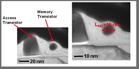 |
| TEM images of ultra-scaled self-aligned split-gate device, with a memory gate length of 16nm. |
Abstract:
CEA-Leti announced today it has fabricated ultra-scaled split-gate memories with gate length of 16nm, and demonstrated their functionality, showing good writing and erasing performances with memory windows over 6V.
Leti Demonstrates Ultra-scaled Self-aligned Split-gate Memory Cell With 16nm Gate Length: Benefits Especially for Contactless Applications Include Larger Memory Window, Improved Control of Spacer Memory Gate Shape and Length, And Better Functionality
Grenoble, France | Posted on March 13th, 2014The devices provide several benefits especially for contactless memory applications, such as enlargement of the memory window and increased functionality. Also because of an optimised fabrication step, the devices allow better control of spacer memory gate shape and length.
Split-gate flash memories are made of two transistors: an access transistor and a memory transistor with a charge-trapping layer (nitride, Si nanocrystals etc.). Split-gate architectures use a low-access voltage and minimize drain current during programming, which leads to a decrease of the programming power compared to standard one-transistor NOR memories. Because programming energy decreases when memory gate length decreases, ultra-scaling is particularly relevant for contactless applications.
Memory gate has been reduced down to 16nm thanks to a poly-Si spacer formed on the sidewall of the select transistor. This approach avoids costly lithography steps during fabrication and solves misalignment issues, which are responsible for a strong variation of the electrical performances, such as the memory window.
The main challenges of this self-aligned technology concern the precise control of the spacer memory gate shape and of the memory gate length. Spacer gate has to fulfil two difficult requirements: being as flat as possible in order to get a silicidation surface as large as possible while insuring a functional contact, and getting a steep edge in order to control the drain-junction doping.
####
About CEA-Leti
By creating innovation and transferring it to industry, Leti is the bridge between basic research and production of micro- and nanotechnologies that improve the lives of people around the world. Backed by its portfolio of 2,200 patents, Leti partners with large industrials, SMEs and startups to tailor advanced solutions that strengthen their competitive positions. It has launched more than 50 startups. Its 8,000m� of new-generation cleanroom space feature 200mm and 300mm wafer processing of micro and nano solutions for applications ranging from space to smart devices. Leti�s staff of more than 1,700 includes 200 assignees from partner companies. Leti is based in Grenoble, France, and has offices in Silicon Valley, Calif., and Tokyo.
For more information, please click here
Contacts:
CEA-Leti
+33 4 38 78 02 26
Agency
+33 6 64 52 81 10
Copyright © CEA-Leti
If you have a comment, please Contact us.Issuers of news releases, not 7th Wave, Inc. or Nanotechnology Now, are solely responsible for the accuracy of the content.
Bookmark:


| Related News Press |
News and information
![]() Quantum computer improves AI predictions April 17th, 2026
Quantum computer improves AI predictions April 17th, 2026
![]() Flexible sensor gains sensitivity under pressure April 17th, 2026
Flexible sensor gains sensitivity under pressure April 17th, 2026
![]() A reusable chip for particulate matter sensing April 17th, 2026
A reusable chip for particulate matter sensing April 17th, 2026
![]() Detecting vibrational quantum beating in the predissociation dynamics of SF6 using time-resolved photoelectron spectroscopy April 17th, 2026
Detecting vibrational quantum beating in the predissociation dynamics of SF6 using time-resolved photoelectron spectroscopy April 17th, 2026
Chip Technology
![]() A reusable chip for particulate matter sensing April 17th, 2026
A reusable chip for particulate matter sensing April 17th, 2026
![]() Metasurfaces smooth light to boost magnetic sensing precision January 30th, 2026
Metasurfaces smooth light to boost magnetic sensing precision January 30th, 2026
Memory Technology
![]() Researchers tackle the memory bottleneck stalling quantum computing October 3rd, 2025
Researchers tackle the memory bottleneck stalling quantum computing October 3rd, 2025
![]() First real-time observation of two-dimensional melting process: Researchers at Mainz University unveil new insights into magnetic vortex structures August 8th, 2025
First real-time observation of two-dimensional melting process: Researchers at Mainz University unveil new insights into magnetic vortex structures August 8th, 2025
![]() Utilizing palladium for addressing contact issues of buried oxide thin film transistors April 5th, 2024
Utilizing palladium for addressing contact issues of buried oxide thin film transistors April 5th, 2024
Announcements
![]() A fundamentally new therapeutic approach to cystic fibrosis: Nanobody repairs cellular defect April 17th, 2026
A fundamentally new therapeutic approach to cystic fibrosis: Nanobody repairs cellular defect April 17th, 2026
![]() UC Irvine physicists discover method to reverse �quantum scrambling� : The work addresses the problem of information loss in quantum computing system April 17th, 2026
UC Irvine physicists discover method to reverse �quantum scrambling� : The work addresses the problem of information loss in quantum computing system April 17th, 2026
|
|
||
|
|
||
| The latest news from around the world, FREE | ||
|
|
||
|
|
||
| Premium Products | ||
|
|
||
|
Only the news you want to read!
Learn More |
||
|
|
||
|
Full-service, expert consulting
Learn More |
||
|
|
||