Home > Press > Ultra-small and Ultra–fast Electro-optic Modulator
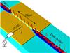 |
| Due to the voltage applied, a beam of light (top left) is modulated by the digital bits (bottom right) of the converter (yellow). An electrical signal is converted into an optical signal. Graphics: A. Melikyan/KIT |
Abstract:
Thanks to optical signals, mails and data can be transmitted rapidly around the globe. But also exchange of digital information between electronic chips may be accelerated and energy efficiency might be increased by using optical signals. However, this would require simple methods to switch from electrical to optical signals. In the Nature Photonics magazine, researchers now present a device of 29 µm in length, which converts signals at a rate of about 40 gigabits per second. It is the most compact high-speed phase modulator in the world. DOI: 10.1038/NPHOTON.2014.9.
Ultra-small and Ultra–fast Electro-optic Modulator
Karlsruhe, Germany | Posted on February 17th, 2014"Conversion of electrical into optical signals happens closer to the processor," Juerg Leuthold says. He coordinated the research project at the Karlsruhe Institute of Technology and has meanwhile moved to the ETH Zurich. "As a result, speed gains are achieved and conduction losses can be prevented. This might reduce energy consumption of the growing information technology."
The electro-optical converter consists of two parallel gold electrodes of about 29 µm in length, which is one third of the diameter of a human hair. The electrodes are separated by a gap of about one tenth of a micrometer in width. The voltage applied to the electrodes is synchronized with the digital data. The gap is filled with an electro-optical polymer, whose refraction index changes as a function of the applied voltage. "A continuous beam of light from the silicon waveguide excites electromagnetic surface waves, so-called surface plasmons (SP), in the gap," Argishti Melikyan, KIT, first author of the publication, explains. "As a result of the voltage applied to the polymer, the phase of the SP is modulated. At the end of the device, the modulated SP enter the exit silicon waveguide in the form of a modulated beam of light. In this way, the data bits are encoded in the phase of the light."
Their recent results revealed that the electro-optic modulator reliably converts data flows of about 40 gigabits per second. It uses the infrared light of 1480 - 1600 nanometers in wavelength usually encountered in the broadband glass fiber network. Even temperatures of up to 85°C do not cause any operation failures. The presented device is the most compact high-speed phase modulator in the world. It can be produced by well-established CMOS fabrication processes. Integration into current chip architectures is hence possible. "The device combines many advantages of other systems, such as a high modulation speed, compact design, and energy efficiency. In the future, plasmonic devices might be used for signal processing in the terahertz range," says Christian Koos, spokesperson of KIT's Helmholtz International Research School of Teratronics (HIRST), which focuses on merging photonic and electronic techniques for high-speed signal processing. "Hundreds of plasmonic modulators might fit on a chip and data rates in the range of terabits per second might be reached."
Presently, information and communication systems consume about 10 percent of the electricity in Germany. This includes computers and smartphones of individual users as well as servers at large computing centers. As data traffic grows exponentially, new approaches are required to increasing the capacity of such systems and reducing their energy consumption at the same time. Plasmonic components might be of decisive importance in this respect.
The present paper is part of the EU project NAVOLCHI, Nano Scale Disruptive Silicon-Plasmonic Platform for Chip-to-Chip Interconnection. This project is aimed at using the interaction of light and electrons in metal surfaces for the development of novel components for data transmission between chips. "Conventional electric chip-to-chip data transmission reaches its limits," says the present project coordinator Manfred Kohl, KIT. "NAVOLCHI is about to overcome those limits using optical technology." It is funded under the 7th Research Framework Programme of the EU and has a budget of EUR 3.4 million.
####
About Karlsruhe Institute of Technology
Karlsruhe Institute of Technology (KIT) is a public corporation according to the legislation of the state of Baden-Württemberg. It fulfills the mission of a university and the mission of a national research center of the Helmholtz Association. Research activities focus on energy, the natural and built environment as well as on society and technology and cover the whole range extending from fundamental aspects to application. With about 9000 employees, including nearly 6000 staff members in the science and education sector, and 24000 students, KIT is one of the biggest research and education institutions in Europe. Work of KIT is based on the knowledge triangle of research, teaching, and innovation.
For more information, please click here
Contacts:
Monika Landgraf
Karlsruhe Institute for Technologie
+49 721 608-47414
For further information
please contact:
Kosta Schinarakis
PKM
Themenscout
Tel.: +49 721 608-41956
Fax: +49 721 608-43568
Copyright © AlphaGalileo
If you have a comment, please Contact us.Issuers of news releases, not 7th Wave, Inc. or Nanotechnology Now, are solely responsible for the accuracy of the content.
Bookmark:


| Related Links |
![]() For more information on the NAVOLCHI project, click:
For more information on the NAVOLCHI project, click:
![]() Full bibliographic information
Full bibliographic information
| Related News Press |
News and information
![]() Quantum computer improves AI predictions April 17th, 2026
Quantum computer improves AI predictions April 17th, 2026
![]() Flexible sensor gains sensitivity under pressure April 17th, 2026
Flexible sensor gains sensitivity under pressure April 17th, 2026
![]() A reusable chip for particulate matter sensing April 17th, 2026
A reusable chip for particulate matter sensing April 17th, 2026
![]() Detecting vibrational quantum beating in the predissociation dynamics of SF6 using time-resolved photoelectron spectroscopy April 17th, 2026
Detecting vibrational quantum beating in the predissociation dynamics of SF6 using time-resolved photoelectron spectroscopy April 17th, 2026
Govt.-Legislation/Regulation/Funding/Policy
![]() Quantum computer improves AI predictions April 17th, 2026
Quantum computer improves AI predictions April 17th, 2026
![]() Metasurfaces smooth light to boost magnetic sensing precision January 30th, 2026
Metasurfaces smooth light to boost magnetic sensing precision January 30th, 2026
![]() New imaging approach transforms study of bacterial biofilms August 8th, 2025
New imaging approach transforms study of bacterial biofilms August 8th, 2025
Chip Technology
![]() A reusable chip for particulate matter sensing April 17th, 2026
A reusable chip for particulate matter sensing April 17th, 2026
![]() Metasurfaces smooth light to boost magnetic sensing precision January 30th, 2026
Metasurfaces smooth light to boost magnetic sensing precision January 30th, 2026
Optical computing/Photonic computing
![]() ICFO researchers overcome long-standing bottleneck in single photon detection with twisted 2D materials August 8th, 2025
ICFO researchers overcome long-standing bottleneck in single photon detection with twisted 2D materials August 8th, 2025
![]() Programmable electron-induced color router array May 14th, 2025
Programmable electron-induced color router array May 14th, 2025
Discoveries
![]() Quantum computer improves AI predictions April 17th, 2026
Quantum computer improves AI predictions April 17th, 2026
![]() Flexible sensor gains sensitivity under pressure April 17th, 2026
Flexible sensor gains sensitivity under pressure April 17th, 2026
![]() A reusable chip for particulate matter sensing April 17th, 2026
A reusable chip for particulate matter sensing April 17th, 2026
![]() Detecting vibrational quantum beating in the predissociation dynamics of SF6 using time-resolved photoelectron spectroscopy April 17th, 2026
Detecting vibrational quantum beating in the predissociation dynamics of SF6 using time-resolved photoelectron spectroscopy April 17th, 2026
Interviews/Book Reviews/Essays/Reports/Podcasts/Journals/White papers/Posters
![]() A fundamentally new therapeutic approach to cystic fibrosis: Nanobody repairs cellular defect April 17th, 2026
A fundamentally new therapeutic approach to cystic fibrosis: Nanobody repairs cellular defect April 17th, 2026
![]() UC Irvine physicists discover method to reverse ‘quantum scrambling’ : The work addresses the problem of information loss in quantum computing system April 17th, 2026
UC Irvine physicists discover method to reverse ‘quantum scrambling’ : The work addresses the problem of information loss in quantum computing system April 17th, 2026
Photonics/Optics/Lasers
![]() Metasurfaces smooth light to boost magnetic sensing precision January 30th, 2026
Metasurfaces smooth light to boost magnetic sensing precision January 30th, 2026
![]() From sensors to smart systems: the rise of AI-driven photonic noses January 30th, 2026
From sensors to smart systems: the rise of AI-driven photonic noses January 30th, 2026
|
|
||
|
|
||
| The latest news from around the world, FREE | ||
|
|
||
|
|
||
| Premium Products | ||
|
|
||
|
Only the news you want to read!
Learn More |
||
|
|
||
|
Full-service, expert consulting
Learn More |
||
|
|
||