Home > Press > A Deeper Look at Interfaces: Researchers at Berkeley Lab’s Advanced Light Source Develop New Technique for Probing Subsurface Electronic Structure
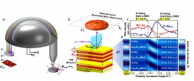 |
| Experimental setup and basic principles of SWARPES shows (a) the experimental setup; (b) diagram of the multilayer STO and LSMO film; (c) SW-excited photoemission intensity rocking curves and (d) simulated intensity of the x-ray standing wave field as a function of depth and grazing incidence angle. |
Abstract:
"The interface is the device," Nobel laureate Herbert Kroemer famously observed, referring to the remarkable properties to be found at the junctures where layers of different materials meet. In today's burgeoning world of nanotechnology, the interfaces between layers of metal oxides are becoming increasingly prominent, with applications in such high-tech favorites as spintronics, high-temperature superconductors, ferroelectrics and multiferroics. Realizing the vast potential of these metal oxide interfaces, especially those buried in subsurface layers, will require detailed knowledge of their electronic structure.
A Deeper Look at Interfaces: Researchers at Berkeley Lab’s Advanced Light Source Develop New Technique for Probing Subsurface Electronic Structure
Berkeley, CA | Posted on January 15th, 2014A new technique from an international team of researchers working at Berkeley Lab's Advanced Light Source (ALS) promises to deliver the goods. In a study led by Charles Fadley, a physicist who holds joint appointments with Berkeley Lab's Materials Sciences Division and the University of California Davis, where he is a Distinguished Professor of Physics, the team combined two well-established techniques for studying electronic structure in crystalline materials into a new technique that is optimized for examining electronic properties at subsurface interfaces. They call this new technique SWARPES, for Standing Wave Angle-Resolved Photoemission Spectroscopy.
"SWARPES allows us for the first time to selectively study buried interfaces with either soft or hard x-rays," Fadley says. "The technique can be applied to any multilayer prototype device structure in spintronics, strongly correlated/high-TC superconductors, or semiconductor electronics. The only limitations are that the sample has to have a high degree of crystalline order, and has to be grown on a nanoscale multilayer mirror suitable for generating an x-ray standing wave."
As the name indicates, SWARPES combines the use of standing waves of x-rays with ARPES, the technique of choice for studying electronic structure. A standing wave is a vibrational pattern created when two waves of identical wavelength interfere with one another: one is the incident x-ray and the other is the x-ray reflected by a mirror. Interactions between standing waves and core-level electrons reveal much about the properties of each atomic species in a sample. ARPES from the outer valence levels is the long-standing spectroscopic workhorse for the study of electronic structure. X-rays striking a material surface or interface cause the photoemission of electrons at angles and kinetic energies that can be measured to obtain detailed electronic energy levels of the sample. While an extremely powerful tool, ARPES, a soft x-ray technique, is primarily limited to the study of near-surface atoms. It's harder x-ray cousin, HARPES, makes use of more energetic x-rays to effectively probe subsurface interfaces, but the addition of the standing wave capability provides a much desired depth selectivity.
"The standing wave can be moved up and down in a sample simply by rocking the angle of incidence around the Bragg angle of the mirror," says Alexander Gray, a former member of Fadley's UC Davis research group and affiliate with Berkeley Lab's Materials Sciences Division, who is now a postdoctoral associate at Stanford/SLAC. "Observing an interface between a ferromagnetic conductor (lanthanum strontium manganite) and an insulator (strontium titanate), which constitute a magnetic tunnel junction used in spintronic logic circuits, we've shown that changes in the electronic structure can be reliably measured, and that these changes are semi-quantitatively predicted by theory at several levels. Our results point to a much wider use of SWARPES in the future for studying the electronic properties of buried interfaces of many different kinds."
Fadley, Gray and their collaborators carried out their SWARPES tests at ALS Beamline 7.0.1. The Advanced Light Source is a U.S. Department of Energy (DOE) national user facility and Beamline 7.0.1 features a premier endstation for determining the electronic structure of metals, semiconductors and insulators. Additional corroborating measurements concerning the interface atomic structure were performed at the National Center for Electron Microscopy (NCEM), another DOE national user facility hosted at Berkeley Lab.
This research was supported primarily by the U.S. Department of Energy (DOE) Office of Science.
####
For more information, please click here
Contacts:
Lynn Yarris
510-486-5375
Copyright © Berkeley Lab
If you have a comment, please Contact us.Issuers of news releases, not 7th Wave, Inc. or Nanotechnology Now, are solely responsible for the accuracy of the content.
Bookmark:


| Related Links |
![]() For more about the research of Charles Fadley, go here:
For more about the research of Charles Fadley, go here:
![]() For more about Berkeley Lab’s Advanced Light Source go here:
For more about Berkeley Lab’s Advanced Light Source go here:
| Related News Press |
News and information
![]() Quantum computer improves AI predictions April 17th, 2026
Quantum computer improves AI predictions April 17th, 2026
![]() Flexible sensor gains sensitivity under pressure April 17th, 2026
Flexible sensor gains sensitivity under pressure April 17th, 2026
![]() A reusable chip for particulate matter sensing April 17th, 2026
A reusable chip for particulate matter sensing April 17th, 2026
![]() Detecting vibrational quantum beating in the predissociation dynamics of SF6 using time-resolved photoelectron spectroscopy April 17th, 2026
Detecting vibrational quantum beating in the predissociation dynamics of SF6 using time-resolved photoelectron spectroscopy April 17th, 2026
Superconductivity
![]() MXene nanomaterials enter a new dimension Multilayer nanomaterial: MXene flakes created at Drexel University show new promise as 1D scrolls January 30th, 2026
MXene nanomaterials enter a new dimension Multilayer nanomaterial: MXene flakes created at Drexel University show new promise as 1D scrolls January 30th, 2026
Govt.-Legislation/Regulation/Funding/Policy
![]() Quantum computer improves AI predictions April 17th, 2026
Quantum computer improves AI predictions April 17th, 2026
![]() Metasurfaces smooth light to boost magnetic sensing precision January 30th, 2026
Metasurfaces smooth light to boost magnetic sensing precision January 30th, 2026
![]() New imaging approach transforms study of bacterial biofilms August 8th, 2025
New imaging approach transforms study of bacterial biofilms August 8th, 2025
Spintronics
![]() Quantum materials: Electron spin measured for the first time June 9th, 2023
Quantum materials: Electron spin measured for the first time June 9th, 2023
Chip Technology
![]() A reusable chip for particulate matter sensing April 17th, 2026
A reusable chip for particulate matter sensing April 17th, 2026
![]() Metasurfaces smooth light to boost magnetic sensing precision January 30th, 2026
Metasurfaces smooth light to boost magnetic sensing precision January 30th, 2026
Discoveries
![]() Quantum computer improves AI predictions April 17th, 2026
Quantum computer improves AI predictions April 17th, 2026
![]() Flexible sensor gains sensitivity under pressure April 17th, 2026
Flexible sensor gains sensitivity under pressure April 17th, 2026
![]() A reusable chip for particulate matter sensing April 17th, 2026
A reusable chip for particulate matter sensing April 17th, 2026
![]() Detecting vibrational quantum beating in the predissociation dynamics of SF6 using time-resolved photoelectron spectroscopy April 17th, 2026
Detecting vibrational quantum beating in the predissociation dynamics of SF6 using time-resolved photoelectron spectroscopy April 17th, 2026
Materials/Metamaterials/Magnetoresistance
![]() First real-time observation of two-dimensional melting process: Researchers at Mainz University unveil new insights into magnetic vortex structures August 8th, 2025
First real-time observation of two-dimensional melting process: Researchers at Mainz University unveil new insights into magnetic vortex structures August 8th, 2025
![]() Researchers unveil a groundbreaking clay-based solution to capture carbon dioxide and combat climate change June 6th, 2025
Researchers unveil a groundbreaking clay-based solution to capture carbon dioxide and combat climate change June 6th, 2025
![]() A 1960s idea inspires NBI researchers to study hitherto inaccessible quantum states June 6th, 2025
A 1960s idea inspires NBI researchers to study hitherto inaccessible quantum states June 6th, 2025
![]() Institute for Nanoscience hosts annual proposal planning meeting May 16th, 2025
Institute for Nanoscience hosts annual proposal planning meeting May 16th, 2025
Announcements
![]() A fundamentally new therapeutic approach to cystic fibrosis: Nanobody repairs cellular defect April 17th, 2026
A fundamentally new therapeutic approach to cystic fibrosis: Nanobody repairs cellular defect April 17th, 2026
![]() UC Irvine physicists discover method to reverse ‘quantum scrambling’ : The work addresses the problem of information loss in quantum computing system April 17th, 2026
UC Irvine physicists discover method to reverse ‘quantum scrambling’ : The work addresses the problem of information loss in quantum computing system April 17th, 2026
Interviews/Book Reviews/Essays/Reports/Podcasts/Journals/White papers/Posters
![]() A fundamentally new therapeutic approach to cystic fibrosis: Nanobody repairs cellular defect April 17th, 2026
A fundamentally new therapeutic approach to cystic fibrosis: Nanobody repairs cellular defect April 17th, 2026
![]() UC Irvine physicists discover method to reverse ‘quantum scrambling’ : The work addresses the problem of information loss in quantum computing system April 17th, 2026
UC Irvine physicists discover method to reverse ‘quantum scrambling’ : The work addresses the problem of information loss in quantum computing system April 17th, 2026
Tools
![]() Metasurfaces smooth light to boost magnetic sensing precision January 30th, 2026
Metasurfaces smooth light to boost magnetic sensing precision January 30th, 2026
![]() From sensors to smart systems: the rise of AI-driven photonic noses January 30th, 2026
From sensors to smart systems: the rise of AI-driven photonic noses January 30th, 2026
![]() Japan launches fully domestically produced quantum computer: Expo visitors to experience quantum computing firsthand August 8th, 2025
Japan launches fully domestically produced quantum computer: Expo visitors to experience quantum computing firsthand August 8th, 2025
|
|
||
|
|
||
| The latest news from around the world, FREE | ||
|
|
||
|
|
||
| Premium Products | ||
|
|
||
|
Only the news you want to read!
Learn More |
||
|
|
||
|
Full-service, expert consulting
Learn More |
||
|
|
||