Home > Press > Park Systems Unveils New Park XE15: Powerfully Versatile Atomic Force Microscope With Unique MultiSampleTM Scan
 |
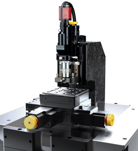
| Park XE15- Powerfully Versatile Atomic Force Microscope With Unique MultiSampleTM Scan |
Abstract:
Park Systems, a leading manufacturer of atomic force microscopy (AFM) products, announces the debut of Park XE15, a powerfully versatile atomic force microscope featuring a unique MultiSampleTM scan. This newly developed large sample AFM provides researchers and operators with the ability to automatically image and measure up to nine individual samples
Park Systems Unveils New Park XE15: Powerfully Versatile Atomic Force Microscope With Unique MultiSampleTM Scan
Santa Clara, CA | Posted on January 6th, 2014Park Systems, a leading manufacturer of atomic force microscopy (AFM) products, announces the debut of Park XE15, a powerfully versatile atomic force microscope featuring a unique MultiSampleTM scan. This newly developed large sample AFM provides researchers and operators with the ability to automatically image and measure up to nine individual samples. Park XE15 can also easily scan larger samples of up to 200 mm x 200 mm, a vast improvement from the current AFM products on the market. Park XE15 is ideally suited for shared labs environments that handle a diverse range of samples, researchers doing multi variant experiments, and failure analysis engineers working on wafers.
"We continue to set new standards of excellence with our new technology and high accuracy in AFM imaging and measurements," says Dr. Sang-Il Park, the founder and CEO of Park Systems. "Park XE15features our most inclusive set of scan modes and can process a range of sample sizes, designed specifically to provide ease of use for shared labs with a wide range of individual requirements."
Park XE15 is the only AFM that maximizes the efficiency of product use with MultiSampleTM scan, automated imaging of multiple samples in one pass. Specially designed multi-sample chuck holds up to nine individual samples which allows operators to scan the samples under identical environmental conditions, improving the accuracy and reliability of the data. After loading the stage with multimple samples, the scan process can be intitated. This makes it ideal for researchers wanting to scan larger samples or failure analysis engineers who need to place silicon wafers on the stage.
"Over the many years that I have worked with Park System, I have found them very responsive to customer feedback in developing new products. Park XE 15 is a problem-solver for engineers who need to process multiple samples simultaneously in a controlled environment," Comments Ahmed A. Busnaina, Professor and Director The NSF Nanoscale Science and Engineering Center for High-rate Nanomanufacturing (NSEC) and the NSF Center for Microcontamination Control, Northeastern University. "The Park engineering team is a great nanoscale partner, working in unisom with customers to create products that meet customer performance requirements."
####
About Park Systems
Park Systems is a world-leading manufacturer of atomic force microscopy (AFM) systems with a complete range of products for researchers and industry engineers in chemistry, materials, physics, life sciences, semiconductor and data storage industries. Park�s products are used by over a thousand institutions and corporations worldwide. Park�s AFM provides highest data accuracy at nanoscale resolution, superior productivity, and lowest operating cost thanks to its unique technology and innovative engineering. Park Systems, Inc. is headquartered in Santa Clara, California with its global manufacturing, and R&D headquarters in Korea. Park�s products are sold and supported worldwide with regional headquarters in the US, Korea, Japan, and Singapore, and distribution partners throughout Europe, Asia, and America. Please visit http://www.parkafm.com or call 408-986-1110 for more information.
For more information, please click here
Contacts:
Debbie West
Phone: 7742780091
Fax: 7742780091
408-986-1110
Copyright © Park Systems
If you have a comment, please Contact us.Issuers of news releases, not 7th Wave, Inc. or Nanotechnology Now, are solely responsible for the accuracy of the content.
| Related News Press |
News and information
![]() Quantum computer improves AI predictions April 17th, 2026
Quantum computer improves AI predictions April 17th, 2026
![]() Flexible sensor gains sensitivity under pressure April 17th, 2026
Flexible sensor gains sensitivity under pressure April 17th, 2026
![]() A reusable chip for particulate matter sensing April 17th, 2026
A reusable chip for particulate matter sensing April 17th, 2026
![]() Detecting vibrational quantum beating in the predissociation dynamics of SF6 using time-resolved photoelectron spectroscopy April 17th, 2026
Detecting vibrational quantum beating in the predissociation dynamics of SF6 using time-resolved photoelectron spectroscopy April 17th, 2026
Imaging
![]() Simple algorithm paired with standard imaging tool could predict failure in lithium metal batteries August 8th, 2025
Simple algorithm paired with standard imaging tool could predict failure in lithium metal batteries August 8th, 2025
Announcements
![]() A fundamentally new therapeutic approach to cystic fibrosis: Nanobody repairs cellular defect April 17th, 2026
A fundamentally new therapeutic approach to cystic fibrosis: Nanobody repairs cellular defect April 17th, 2026
![]() UC Irvine physicists discover method to reverse �quantum scrambling� : The work addresses the problem of information loss in quantum computing system April 17th, 2026
UC Irvine physicists discover method to reverse �quantum scrambling� : The work addresses the problem of information loss in quantum computing system April 17th, 2026
Tools
![]() Metasurfaces smooth light to boost magnetic sensing precision January 30th, 2026
Metasurfaces smooth light to boost magnetic sensing precision January 30th, 2026
![]() From sensors to smart systems: the rise of AI-driven photonic noses January 30th, 2026
From sensors to smart systems: the rise of AI-driven photonic noses January 30th, 2026
![]() Japan launches fully domestically produced quantum computer: Expo visitors to experience quantum computing firsthand August 8th, 2025
Japan launches fully domestically produced quantum computer: Expo visitors to experience quantum computing firsthand August 8th, 2025
|
|
||
|
|
||
| The latest news from around the world, FREE | ||
|
|
||
|
|
||
| Premium Products | ||
|
|
||
|
Only the news you want to read!
Learn More |
||
|
|
||
|
Full-service, expert consulting
Learn More |
||
|
|
||


