Home > Press > Penn Researchers Grow Liquid Crystal 'Flowers' That Can Be Used as Lenses
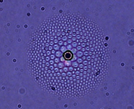 |
| A liquid crystal "flower" under magnification. The black dot at center is the silica bead that generates the flower's pattern. |
Abstract:
A team of material scientists, chemical engineers and physicists from the University of Pennsylvania has made another advance in their effort to use liquid crystals as a medium for assembling structures.
Penn Researchers Grow Liquid Crystal 'Flowers' That Can Be Used as Lenses
Philadelphia, PA | Posted on December 20th, 2013In their earlier studies, the team produced patterns of "defects," useful disruptions in the repeating patterns found in liquid crystals, in nanoscale grids and rings. The new study adds a more complex pattern out of an even simpler template: a three-dimensional array in the shape of a flower.
And because the petals of this "flower" are made of transparent liquid crystal and radiate out in a circle from a central point, the ensemble resembles a compound eye and can thus be used as a lens.
The team consists of Randall Kamien, professor in the School of Arts and Sciences' Department of Physics and Astronomy; Kathleen Stebe, the School of Engineering and Applied Science's deputy dean for research and professor in Chemical and Biomolecular Engineering and Shu Yang, professor in Engineering's departments of Materials Science and Engineering and Chemical and Biomolecular Engineering. Members of their labs also contributed to the new study, including lead author Daniel Beller, Mohamed Gharbi and Apiradee Honglawan.
Their work was published in Physical Review X.
The researchers' ongoing work with liquid crystals is an example of a growing field of nanotechnology known as "directed assembly," in which scientists and engineers aim to manufacture structures on the smallest scales without having to individually manipulate each component. Rather, they set out precisely defined starting conditions and let the physics and chemistry that govern those components do the rest.
The starting conditions in the researchers previous experiments were templates consisting of tiny posts. In one of their studies, they showed that changing the size, shape or spacing of these posts would result in corresponding changes in the patterns of defects on the surface of the liquid crystal resting on top of them. In another experiment, they showed they could make a "hula hoop" of defects around individual posts, which would then act as a second template for a ring of defects at the surface.
In their latest work, the researchers used a much simpler cue.
"Before we were growing these liquid crystals on something like a trellis, a template with precisely ordered features," Kamien said. "Here, we're just planting a seed."
The seed, in this case, were silica beads � essentially, polished grains of sand. Planted at the top of a pool of liquid crystal flower-like patterns of defects grow around each bead.
The key difference between the template in this experiment and ones in the research team's earlier work was the shape of the interface between the template and the liquid crystal.
In their experiment that generated grid patterns of defects, those patterns stemmed from cues generated by the templates' microposts. Domains of elastic energy originated on the flat tops and edges of these posts and travelled up the liquid crystal's layers, culminating in defects. Using a bead instead of a post, as the researchers did in their latest experiment, makes it so that the interface is no longer flat.
"Not only is the interface at an angle, it's an angle that keeps changing," Kamien said. "The way the liquid crystal responds to that is that it makes these petal-like shapes at smaller and smaller sizes, trying to match the angle of the bead until everything is flat."
Surface tension on the bead also makes it so these petals are arranged in a tiered, convex fashion. And because the liquid crystal can interact with light, the entire assembly can function as a lens, focusing light to a point underneath the bead.
"It's like an insect's compound eye, or the mirrors on the biggest telescopes," said Kamien. "As we learn more about these systems, we're going to be able to make these kinds of lenses to order and use them to direct light."
This type of directed assembly could be useful in making optical switches and in other applications.
The research was supported by the National Science Foundation, Penn's Materials Science Research and Engineering Center and the Simons Foundation.
####
For more information, please click here
Contacts:
Evan Lerner
215-573-6604
Copyright © University of Pennsylvania
If you have a comment, please Contact us.Issuers of news releases, not 7th Wave, Inc. or Nanotechnology Now, are solely responsible for the accuracy of the content.
Bookmark:


| Related Links |
| Related News Press |
News and information
![]() Quantum computer improves AI predictions April 17th, 2026
Quantum computer improves AI predictions April 17th, 2026
![]() Flexible sensor gains sensitivity under pressure April 17th, 2026
Flexible sensor gains sensitivity under pressure April 17th, 2026
![]() A reusable chip for particulate matter sensing April 17th, 2026
A reusable chip for particulate matter sensing April 17th, 2026
![]() Detecting vibrational quantum beating in the predissociation dynamics of SF6 using time-resolved photoelectron spectroscopy April 17th, 2026
Detecting vibrational quantum beating in the predissociation dynamics of SF6 using time-resolved photoelectron spectroscopy April 17th, 2026
Display technology/LEDs/SS Lighting/OLEDs
![]() Spinel-type sulfide semiconductors to operate the next-generation LEDs and solar cells For solar-cell absorbers and green-LED source October 3rd, 2025
Spinel-type sulfide semiconductors to operate the next-generation LEDs and solar cells For solar-cell absorbers and green-LED source October 3rd, 2025
![]() Efficient and stable hybrid perovskite-organic light-emitting diodes with external quantum efficiency exceeding 40 per cent July 5th, 2024
Efficient and stable hybrid perovskite-organic light-emitting diodes with external quantum efficiency exceeding 40 per cent July 5th, 2024
Govt.-Legislation/Regulation/Funding/Policy
![]() Quantum computer improves AI predictions April 17th, 2026
Quantum computer improves AI predictions April 17th, 2026
![]() Metasurfaces smooth light to boost magnetic sensing precision January 30th, 2026
Metasurfaces smooth light to boost magnetic sensing precision January 30th, 2026
![]() New imaging approach transforms study of bacterial biofilms August 8th, 2025
New imaging approach transforms study of bacterial biofilms August 8th, 2025
Molecular Nanotechnology
![]() Quantum pumping in molecular junctions August 16th, 2024
Quantum pumping in molecular junctions August 16th, 2024
![]() Scientists push the boundaries of manipulating light at the submicroscopic level March 3rd, 2023
Scientists push the boundaries of manipulating light at the submicroscopic level March 3rd, 2023
![]() First electric nanomotor made from DNA material: Synthetic rotary motors at the nanoscale perform mechanical work July 22nd, 2022
First electric nanomotor made from DNA material: Synthetic rotary motors at the nanoscale perform mechanical work July 22nd, 2022
Optical computing/Photonic computing
![]() ICFO researchers overcome long-standing bottleneck in single photon detection with twisted 2D materials August 8th, 2025
ICFO researchers overcome long-standing bottleneck in single photon detection with twisted 2D materials August 8th, 2025
![]() Programmable electron-induced color router array May 14th, 2025
Programmable electron-induced color router array May 14th, 2025
Discoveries
![]() Quantum computer improves AI predictions April 17th, 2026
Quantum computer improves AI predictions April 17th, 2026
![]() Flexible sensor gains sensitivity under pressure April 17th, 2026
Flexible sensor gains sensitivity under pressure April 17th, 2026
![]() A reusable chip for particulate matter sensing April 17th, 2026
A reusable chip for particulate matter sensing April 17th, 2026
![]() Detecting vibrational quantum beating in the predissociation dynamics of SF6 using time-resolved photoelectron spectroscopy April 17th, 2026
Detecting vibrational quantum beating in the predissociation dynamics of SF6 using time-resolved photoelectron spectroscopy April 17th, 2026
Announcements
![]() A fundamentally new therapeutic approach to cystic fibrosis: Nanobody repairs cellular defect April 17th, 2026
A fundamentally new therapeutic approach to cystic fibrosis: Nanobody repairs cellular defect April 17th, 2026
![]() UC Irvine physicists discover method to reverse �quantum scrambling� : The work addresses the problem of information loss in quantum computing system April 17th, 2026
UC Irvine physicists discover method to reverse �quantum scrambling� : The work addresses the problem of information loss in quantum computing system April 17th, 2026
Interviews/Book Reviews/Essays/Reports/Podcasts/Journals/White papers/Posters
![]() A fundamentally new therapeutic approach to cystic fibrosis: Nanobody repairs cellular defect April 17th, 2026
A fundamentally new therapeutic approach to cystic fibrosis: Nanobody repairs cellular defect April 17th, 2026
![]() UC Irvine physicists discover method to reverse �quantum scrambling� : The work addresses the problem of information loss in quantum computing system April 17th, 2026
UC Irvine physicists discover method to reverse �quantum scrambling� : The work addresses the problem of information loss in quantum computing system April 17th, 2026
Photonics/Optics/Lasers
![]() Metasurfaces smooth light to boost magnetic sensing precision January 30th, 2026
Metasurfaces smooth light to boost magnetic sensing precision January 30th, 2026
![]() From sensors to smart systems: the rise of AI-driven photonic noses January 30th, 2026
From sensors to smart systems: the rise of AI-driven photonic noses January 30th, 2026
|
|
||
|
|
||
| The latest news from around the world, FREE | ||
|
|
||
|
|
||
| Premium Products | ||
|
|
||
|
Only the news you want to read!
Learn More |
||
|
|
||
|
Full-service, expert consulting
Learn More |
||
|
|
||