Home > Press > Imec Integrates CCD and CMOS Technology to Improve Performance of CMOS imagers
 |
Abstract:
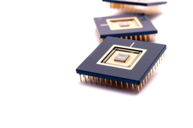
Imec, the Belgian nanoelectronics research center, will present at this week's ‘CMOS Image Sensors for High Performance Applications' workshop in Toulouse (France) a prototype of a high-performance, time-delay-integration (TDI) image sensor. The image sensor is based on imec's proprietary embedded charge-coupled device (CCD) in CMOS technology. Imec developed and fabricated the sensor for the French Space Agency, CNES, which plans to utilize the technology for space-based earth observation.
Imec Integrates CCD and CMOS Technology to Improve Performance of CMOS imagers
Leuven, Belgium | Posted on November 25th, 2013The prototype image sensor combines a light-sensitive, CCD-based TDI pixel array with peripheral CMOS readout electronics. By integrating CCD with CMOS technology, imec combined the best of both worlds. The CCD pixel structure delivers low-noise TDI performance in the charge domain, while CMOS technology enables low-power, on-chip integration of fast and complex circuitry readouts.
A TDI imager is a linear device that utilizes a clever synchronization of the linear motion of the scene with multiple samplings of the same image, thereby increasing the signal to noise ratio. CCDs fit extremely well with the TDI application since they operate in the charge domain, enabling the movement of charges without creating excess noise. By combining the TDI pixels array with CMOS readout circuitry on the same die, imec produced a camera-on-a-chip or system-on-a-chip (SOC) imager, which reduces the overall system complexity and cost. The CMOS technology enables on-chip readout electronics, such as clock drivers and analog-to-digital convertors (ADCs), operating at higher speeds and lower power consumption not possible with traditional CCD technology.
The prototypes were fabricated using imec's 130nm process with an additional CCD process module. An excellent charge transfer efficiency of 99.9987 % has been measured ensuring almost lossless transport of charges in the TDI array, and guaranteeing high image quality. Imec's specialty imaging platform combines custom design (i.e., specialized pixels, high-performance readout circuits and chip architectures) with optimized silicon processing, such as dedicated implants and backside thinning, to achieve high-end specialized imagers.
####
About IMEC
Imec performs world-leading research in nanoelectronics. Imec leverages its scientific knowledge with the innovative power of its global partnerships in ICT, healthcare and energy. Imec delivers industry-relevant technology solutions. In a unique high-tech environment, its international top talent is committed to providing the building blocks for a better life in a sustainable society. Imec is headquartered in Leuven, Belgium, and has offices in Belgium, the Netherlands, Taiwan, US, China, India and Japan. Its staff of close to 2,000 people includes more than 600 industrial residents and guest researchers. In 2011, imec's revenue (P&L) was about 300 million euro. Further information on imec can be found at www.imec.be.
Imec is a registered trademark for the activities of IMEC International (a legal entity set up under Belgian law as a "stichting van openbaar nut”), imec Belgium (IMEC vzw supported by the Flemish Government), imec the Netherlands (Stichting IMEC Nederland, part of Holst Centre which is supported by the Dutch Government), imec Taiwan (IMEC Taiwan Co.) and imec China (IMEC Microelectronics (Shanghai) Co. Ltd.) and imec India (Imec India Private Limited).
For more information, please click here
Contacts:
Hanne Degans
External communications officer
T: +32 16 28 17 69
Mobile: +32 486 065 175
Copyright © IMEC
If you have a comment, please Contact us.Issuers of news releases, not 7th Wave, Inc. or Nanotechnology Now, are solely responsible for the accuracy of the content.
Bookmark:


| Related News Press |
News and information
![]() Quantum computer improves AI predictions April 17th, 2026
Quantum computer improves AI predictions April 17th, 2026
![]() Flexible sensor gains sensitivity under pressure April 17th, 2026
Flexible sensor gains sensitivity under pressure April 17th, 2026
![]() A reusable chip for particulate matter sensing April 17th, 2026
A reusable chip for particulate matter sensing April 17th, 2026
![]() Detecting vibrational quantum beating in the predissociation dynamics of SF6 using time-resolved photoelectron spectroscopy April 17th, 2026
Detecting vibrational quantum beating in the predissociation dynamics of SF6 using time-resolved photoelectron spectroscopy April 17th, 2026
Imaging
![]() Simple algorithm paired with standard imaging tool could predict failure in lithium metal batteries August 8th, 2025
Simple algorithm paired with standard imaging tool could predict failure in lithium metal batteries August 8th, 2025
Govt.-Legislation/Regulation/Funding/Policy
![]() Quantum computer improves AI predictions April 17th, 2026
Quantum computer improves AI predictions April 17th, 2026
![]() Metasurfaces smooth light to boost magnetic sensing precision January 30th, 2026
Metasurfaces smooth light to boost magnetic sensing precision January 30th, 2026
![]() New imaging approach transforms study of bacterial biofilms August 8th, 2025
New imaging approach transforms study of bacterial biofilms August 8th, 2025
Sensors
![]() Flexible sensor gains sensitivity under pressure April 17th, 2026
Flexible sensor gains sensitivity under pressure April 17th, 2026
![]() Tiny nanosheets, big leap: A new sensor detects ethanol at ultra-low levels January 30th, 2026
Tiny nanosheets, big leap: A new sensor detects ethanol at ultra-low levels January 30th, 2026
![]() From sensors to smart systems: the rise of AI-driven photonic noses January 30th, 2026
From sensors to smart systems: the rise of AI-driven photonic noses January 30th, 2026
![]() Sensors innovations for smart lithium-based batteries: advancements, opportunities, and potential challenges August 8th, 2025
Sensors innovations for smart lithium-based batteries: advancements, opportunities, and potential challenges August 8th, 2025
Announcements
![]() A fundamentally new therapeutic approach to cystic fibrosis: Nanobody repairs cellular defect April 17th, 2026
A fundamentally new therapeutic approach to cystic fibrosis: Nanobody repairs cellular defect April 17th, 2026
![]() UC Irvine physicists discover method to reverse ‘quantum scrambling’ : The work addresses the problem of information loss in quantum computing system April 17th, 2026
UC Irvine physicists discover method to reverse ‘quantum scrambling’ : The work addresses the problem of information loss in quantum computing system April 17th, 2026
Aerospace/Space
![]() Decoding hydrogen‑bond network of electrolyte for cryogenic durable aqueous zinc‑ion batteries January 30th, 2026
Decoding hydrogen‑bond network of electrolyte for cryogenic durable aqueous zinc‑ion batteries January 30th, 2026
![]() ICFO researchers overcome long-standing bottleneck in single photon detection with twisted 2D materials August 8th, 2025
ICFO researchers overcome long-standing bottleneck in single photon detection with twisted 2D materials August 8th, 2025
![]() Onion-like nanoparticles found in aircraft exhaust May 14th, 2025
Onion-like nanoparticles found in aircraft exhaust May 14th, 2025
Events/Classes
![]() Institute for Nanoscience hosts annual proposal planning meeting May 16th, 2025
Institute for Nanoscience hosts annual proposal planning meeting May 16th, 2025
![]() A New Blue: Mysterious origin of the ribbontail ray’s electric blue spots revealed July 5th, 2024
A New Blue: Mysterious origin of the ribbontail ray’s electric blue spots revealed July 5th, 2024
![]() Researchers demonstrate co-propagation of quantum and classical signals: Study shows that quantum encryption can be implemented in existing fiber networks January 20th, 2023
Researchers demonstrate co-propagation of quantum and classical signals: Study shows that quantum encryption can be implemented in existing fiber networks January 20th, 2023
|
|
||
|
|
||
| The latest news from around the world, FREE | ||
|
|
||
|
|
||
| Premium Products | ||
|
|
||
|
Only the news you want to read!
Learn More |
||
|
|
||
|
Full-service, expert consulting
Learn More |
||
|
|
||