Home > Press > Riding an electron wave into the future of microchip fabrication: Computer simulation explores how intense plasma waves generate suprathermal electrons, which are critical to microchip fabrication
 |
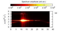
| A plasma wave can give rise to a population of suprathermal electrons.
Credit: I.D. Kaganovich and D. Sydorenko |
Abstract:
Advanced plasma-based etching is a key enabler of Moore's Law that observes that the number of transistors on integrated circuits doubles nearly every two years. It is the plasma's ability to reproduce fine patterns on silicon that makes this scaling possible and has made plasma sources ubiquitous in microchip manufacturing.
Riding an electron wave into the future of microchip fabrication: Computer simulation explores how intense plasma waves generate suprathermal electrons, which are critical to microchip fabrication
College Park, MD | Posted on November 13th, 2013A groundbreaking fabrication technique, based on what is called a DC-augmented capacitively coupled plasma source, affords chip makers unprecedented control of the plasma. This process enables DC-electrode borne electron beams to reach and harden the surface of the mask that is used for printing the microchip circuits. More importantly, the presence of the beam creates a population of suprathermal electrons in the plasma, producing the plasma chemistry that is necessary to protect the mask. The energy of these electrons is greater than simple thermal heating could produce�hence the name "suprathermal." But how the beam electrons transform themselves into this suprathermal population has been a puzzle.
Now a computer simulation developed at the U.S. Department of Energy's Princeton
Plasma Physics Laboratory in collaboration with the University of Alberta has shed light on this transformation. The simulation reveals that the initial DC-electrode borne beam generates intense plasma waves that move through the plasma like ripples in water. And it is this beam-plasma instability that leads to the generation of the crucial suprathermal electrons.
Understanding the role these instabilities play provides a first step toward still-greater control of the plasma-surface interactions, and toward further increasing the number of transistors on integrated circuits. Insights from both numerical simulations and experiments related to beam-plasma instabilities thus portend the development of new plasma sources and the increasingly advanced chips that they fabricate.
Abstracts:
TO6.00005 Collisionless acceleration of plasma electrons by intense electron beam
Session: Low Temperature Plasma Science, Engineering and Technology
9:30 AM-11:06 AM, Thursday, November 14, 2013
####
For more information, please click here
Contacts:
Research Contacts:
I.D. Kaganovich:
(609) 243-3277
D. Sydorenko
University of Alberta
Edmonton, Canada
James Riordon
301-209-3238
American Physical Society
Copyright © American Physical Society
If you have a comment, please Contact us.Issuers of news releases, not 7th Wave, Inc. or Nanotechnology Now, are solely responsible for the accuracy of the content.
| Related News Press |
News and information
![]() Decoding hydrogen‑bond network of electrolyte for cryogenic durable aqueous zinc‑ion batteries January 30th, 2026
Decoding hydrogen‑bond network of electrolyte for cryogenic durable aqueous zinc‑ion batteries January 30th, 2026
![]() COF scaffold membrane with gate‑lane nanostructure for efficient Li+/Mg2+ separation January 30th, 2026
COF scaffold membrane with gate‑lane nanostructure for efficient Li+/Mg2+ separation January 30th, 2026
Chip Technology
![]() Metasurfaces smooth light to boost magnetic sensing precision January 30th, 2026
Metasurfaces smooth light to boost magnetic sensing precision January 30th, 2026
![]() Beyond silicon: Electronics at the scale of a single molecule January 30th, 2026
Beyond silicon: Electronics at the scale of a single molecule January 30th, 2026
![]() Lab to industry: InSe wafer-scale breakthrough for future electronics August 8th, 2025
Lab to industry: InSe wafer-scale breakthrough for future electronics August 8th, 2025
Discoveries
![]() From sensors to smart systems: the rise of AI-driven photonic noses January 30th, 2026
From sensors to smart systems: the rise of AI-driven photonic noses January 30th, 2026
![]() Decoding hydrogen‑bond network of electrolyte for cryogenic durable aqueous zinc‑ion batteries January 30th, 2026
Decoding hydrogen‑bond network of electrolyte for cryogenic durable aqueous zinc‑ion batteries January 30th, 2026
![]() COF scaffold membrane with gate‑lane nanostructure for efficient Li+/Mg2+ separation January 30th, 2026
COF scaffold membrane with gate‑lane nanostructure for efficient Li+/Mg2+ separation January 30th, 2026
Announcements
![]() Decoding hydrogen‑bond network of electrolyte for cryogenic durable aqueous zinc‑ion batteries January 30th, 2026
Decoding hydrogen‑bond network of electrolyte for cryogenic durable aqueous zinc‑ion batteries January 30th, 2026
![]() COF scaffold membrane with gate‑lane nanostructure for efficient Li+/Mg2+ separation January 30th, 2026
COF scaffold membrane with gate‑lane nanostructure for efficient Li+/Mg2+ separation January 30th, 2026
Interviews/Book Reviews/Essays/Reports/Podcasts/Journals/White papers/Posters
![]() Metasurfaces smooth light to boost magnetic sensing precision January 30th, 2026
Metasurfaces smooth light to boost magnetic sensing precision January 30th, 2026
![]() COF scaffold membrane with gate‑lane nanostructure for efficient Li+/Mg2+ separation January 30th, 2026
COF scaffold membrane with gate‑lane nanostructure for efficient Li+/Mg2+ separation January 30th, 2026
Industrial
![]() Tiny nanosheets, big leap: A new sensor detects ethanol at ultra-low levels January 30th, 2026
Tiny nanosheets, big leap: A new sensor detects ethanol at ultra-low levels January 30th, 2026
![]() Quantum interference in molecule-surface collisions February 28th, 2025
Quantum interference in molecule-surface collisions February 28th, 2025
![]() Boron nitride nanotube fibers get real: Rice lab creates first heat-tolerant, stable fibers from wet-spinning process June 24th, 2022
Boron nitride nanotube fibers get real: Rice lab creates first heat-tolerant, stable fibers from wet-spinning process June 24th, 2022
|
|
||
|
|
||
| The latest news from around the world, FREE | ||
|
|
||
|
|
||
| Premium Products | ||
|
|
||
|
Only the news you want to read!
Learn More |
||
|
|
||
|
Full-service, expert consulting
Learn More |
||
|
|
||


