Home > Press > New Extended Pressure SEM from JEOL
 |
Abstract:
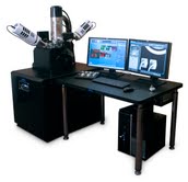
JEOL introduces a new Scanning Electron Microscope with expanded pressure range, large specimen chamber, and unsurpassed resolution for imaging and characterizing a wide variety of sample types and sizes. The JSM-IT300LV is the latest addition to JEOL's popular series of tungsten low vacuum SEMs. This all-new design builds upon the award-winning platform of the company's InTouchScope™, analytical SEM with intuitive touch screen control, and the widely used high-performance analytical SEM, the JSM-6610LV.
New Extended Pressure SEM from JEOL
Peabody, MA | Posted on September 5th, 2013The new JSM-IT300LV extends vacuum pressure range to 10-650pA - more than twice that of earlier models. In low vacuum mode, this capability enhances SEM imaging versatility for samples that are wet, oily, outgas excessively or are non-conductive without pretreatment.
A highly customizable SEM, the JSM-IT300LV features multiple ports for analytical attachments such as: energy dispersive X-ray spectrometer (EDS), electron backscatter diffraction (EBSD), cathodoluminescence detectors (CL), wavelength dispersive X-ray spectrometer (WDS), chamberscopes, heating/cooling substages etc.
The large vacuum chamber accommodates samples up to 300mm in diameter and 80mm in height. When maintaining sample integrity is important, this feature makes it possible to image samples as large as a tennis shoe, automobile part, or full sized silicon wafer without alteration. A variety of sample holders are available for every type of sample including special requirements.
JEOL SEMs are designed for the ultimate user experience and ease of use, and now the choice of multi-touch screen operation as well as keyboard/mouse and knob control will suit a wide variety of users. Sample navigation control, an embedded CCD camera, and 5-axis stage control with even faster asynchronous movement make it possible to image and analyze samples at a wide range of angles and orientations with pinpoint accuracy and location.
Versatility and amazing clarity in imaging across the magnification range of 5X - 300,000X are the hallmarks of the JEOL tungsten SEM family, and the JSM-IT300LV brings that capability to its highest level of performance today.
For more information on the JSM-iT300LV SEM, please visit our web page: www.jeolusa.com/PRODUCTS/ElectronOptics/ScanningElectronMicroscopes(SEM)/HVLVTungstenLaB6SEMs/JSMIT300LV/tabid/1243/Default.aspx
####
For more information, please click here
Copyright © JEOL
If you have a comment, please Contact us.Issuers of news releases, not 7th Wave, Inc. or Nanotechnology Now, are solely responsible for the accuracy of the content.
| Related News Press |
News and information
![]() Quantum computer improves AI predictions April 17th, 2026
Quantum computer improves AI predictions April 17th, 2026
![]() Flexible sensor gains sensitivity under pressure April 17th, 2026
Flexible sensor gains sensitivity under pressure April 17th, 2026
![]() A reusable chip for particulate matter sensing April 17th, 2026
A reusable chip for particulate matter sensing April 17th, 2026
![]() Detecting vibrational quantum beating in the predissociation dynamics of SF6 using time-resolved photoelectron spectroscopy April 17th, 2026
Detecting vibrational quantum beating in the predissociation dynamics of SF6 using time-resolved photoelectron spectroscopy April 17th, 2026
Imaging
![]() Simple algorithm paired with standard imaging tool could predict failure in lithium metal batteries August 8th, 2025
Simple algorithm paired with standard imaging tool could predict failure in lithium metal batteries August 8th, 2025
Announcements
![]() A fundamentally new therapeutic approach to cystic fibrosis: Nanobody repairs cellular defect April 17th, 2026
A fundamentally new therapeutic approach to cystic fibrosis: Nanobody repairs cellular defect April 17th, 2026
![]() UC Irvine physicists discover method to reverse ‘quantum scrambling’ : The work addresses the problem of information loss in quantum computing system April 17th, 2026
UC Irvine physicists discover method to reverse ‘quantum scrambling’ : The work addresses the problem of information loss in quantum computing system April 17th, 2026
Tools
![]() Metasurfaces smooth light to boost magnetic sensing precision January 30th, 2026
Metasurfaces smooth light to boost magnetic sensing precision January 30th, 2026
![]() From sensors to smart systems: the rise of AI-driven photonic noses January 30th, 2026
From sensors to smart systems: the rise of AI-driven photonic noses January 30th, 2026
![]() Japan launches fully domestically produced quantum computer: Expo visitors to experience quantum computing firsthand August 8th, 2025
Japan launches fully domestically produced quantum computer: Expo visitors to experience quantum computing firsthand August 8th, 2025
|
|
||
|
|
||
| The latest news from around the world, FREE | ||
|
|
||
|
|
||
| Premium Products | ||
|
|
||
|
Only the news you want to read!
Learn More |
||
|
|
||
|
Full-service, expert consulting
Learn More |
||
|
|
||


