Home > Press > Device for capturing signatures uses tiny LEDs created with piezo-phototronic effect: Your signature in lights
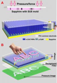 |
| This schematic shows a device for imaging pressure distribution by the piezo-phototronic effect. The illustration shows a nanowire-LED based pressure sensor array before (a) and after (b) applying a compressive strain. A convex character pattern, such as "ABC," molded on a sapphire substrate, is used to apply the pressure pattern on the top of the indium-tin oxide (ITO) electrode.
Credit: Courtesy of Zhong Lin Wang |
Abstract:
Researchers at the Georgia Institute of Technology want to put your signature up in lights - tiny lights, that is. Using thousands of nanometer-scale wires, the researchers have developed a sensor device that converts mechanical pressure - from a signature or a fingerprint - directly into light signals that can be captured and processed optically.
Device for capturing signatures uses tiny LEDs created with piezo-phototronic effect: Your signature in lights
Atlanta, GA | Posted on August 12th, 2013The sensor device could provide an artificial sense of touch, offering sensitivity comparable to that of the human skin. Beyond collecting signatures and fingerprints, the technique could also be used in biological imaging and micro-electromechanical (MEMS) systems. Ultimately, it could provide a new approach for human-machine interfaces.
"You can write with your pen and the sensor will optically detect what you write at high resolution and with a very fast response rate," said Zhong Lin Wang, Regents' professor and Hightower Chair in the School of Materials Science and Engineering at Georgia Tech. "This is a new principle for imaging force that uses parallel detection and avoids many of the complications of existing pressure sensors."
Individual zinc oxide (ZnO) nanowires that are part of the device operate as tiny light emitting diodes (LEDS) when placed under strain from the mechanical pressure, allowing the device to provide detailed information about the amount of pressure being applied. Known as piezo-phototronics, the technology - first described by Wang in 2009 - provides a new way to capture information about pressure applied at very high resolution: up to 6,300 dots per inch.
The research was scheduled to be reported August 11 in the journal Nature Photonics. It was sponsored by the U.S. Department of Energy's Office of Basic Energy Sciences, the National Science Foundation, and the Knowledge Innovation Program of the Chinese Academy of Sciences.
Piezoelectric materials generate a charge polarization when they are placed under strain. The piezo-phototronic devices rely on that physical principle to tune and control the charge transport and recombination by the polarization charges present at the ends of individual nanowires. Grown atop a gallium nitride (GaN) film, the nanowires create pixeled light emitters whose output varies with the pressure, creating an electroluminescent signal that can be integrated with on-chip photonics for data transmission, processing and recording.
"When you have a zinc oxide nanowire under strain, you create a piezoelectric charge at both ends which forms a piezoelectric potential," Wang explained. "The presence of the potential distorts the band structure in the wire, causing electrons to remain in the p-n junction longer and enhancing the efficiency of the LED."
The efficiency increase in the LED is proportional to the strain created. Differences in the amount of strain applied translate to differences in light emitted from the root where the nanowires contact the gallium nitride film.
To fabricate the devices, a low-temperature chemical growth technique is used to create a patterned array of zinc oxide nanowires on a gallium nitride thin film substrate with the c-axis pointing upward. The interfaces between the nanowires and the gallium nitride film form the bottom surfaces of the nanowires. After infiltrating the space between nanowires with a PMMA thermoplastic, oxygen plasma is used to etch away the PMMA enough to expose the tops of the zinc oxide nanowires.
A nickel-gold electrode is then used to form ohmic contact with the bottom gallium-nitride film, and a transparent indium-tin oxide (ITO) film is deposited on the top of the array to serve as a common electrode.
When pressure is applied to the device through handwriting, nanowires are compressed along their axial directions, creating a negative piezo-potential, while uncompressed nanowires have no potential.
The researchers have pressed letters into the top of the device, which produces a corresponding light output from the bottom of the device. This output - which can all be read at the same time - can be processed and transmitted.
The ability to see all of the emitters simultaneously allows the device to provide a quick response. "The response time is fast, and you can read a million pixels in a microsecond," said Wang. "When the light emission is created, it can be detected immediately with the optical fiber."
The nanowires stop emitting light when the pressure is relieved. Switching from one mode to the other takes 90 milliseconds or less, Wang said.
The researchers studied the stability and reproducibility of the sensor array by examining the light emitting intensity of the individual pixels under strain for 25 repetitive on-off cycles. They found that the output fluctuation was approximately five percent, much smaller than the overall level of the signal. The robustness of more than 20,000 pixels was studied.
A spatial resolution of 2.7 microns was recorded from the device samples tested so far. Wang believes the resolution could be improved by reducing the diameter of the nanowires - allowing more nanowires to be grown - and by using a high-temperature fabrication process.
In addition to Wang, the research team also included Caofeng Pan, Lin Dong, Guang Zhu, Simiao Niu, Ruomeng Yo, Qing Yang and Ying Liu, all associated with Georgia Tech. In addition, Pan is associated with the Beijing Institute of Nanoenergy and Nanosystems in the Chinese Academy of Sciences.
This research was supported by the U.S. Department of Energy (DOE), Office of Basic Energy Sciences, Division of Materials Sciences and Engineering under Award DE-FG02-07ER46394; the National Science Foundation (NSF) under award CMMI-040367; and by the Knowledge Innovation program of the Chinese Academy of Sciences under KJCX2-YW-M13. The opinions and conclusions expressed are those of the authors and do not necessarily represent the official views of the DOE or NSF.
####
For more information, please click here
Contacts:
John Toon
404-894-6986
Copyright © Georgia Institute of Technology
If you have a comment, please Contact us.Issuers of news releases, not 7th Wave, Inc. or Nanotechnology Now, are solely responsible for the accuracy of the content.
Bookmark:


| Related News Press |
News and information
![]() Quantum computer improves AI predictions April 17th, 2026
Quantum computer improves AI predictions April 17th, 2026
![]() Flexible sensor gains sensitivity under pressure April 17th, 2026
Flexible sensor gains sensitivity under pressure April 17th, 2026
![]() A reusable chip for particulate matter sensing April 17th, 2026
A reusable chip for particulate matter sensing April 17th, 2026
![]() Detecting vibrational quantum beating in the predissociation dynamics of SF6 using time-resolved photoelectron spectroscopy April 17th, 2026
Detecting vibrational quantum beating in the predissociation dynamics of SF6 using time-resolved photoelectron spectroscopy April 17th, 2026
Imaging
![]() Simple algorithm paired with standard imaging tool could predict failure in lithium metal batteries August 8th, 2025
Simple algorithm paired with standard imaging tool could predict failure in lithium metal batteries August 8th, 2025
![]() First real-time observation of two-dimensional melting process: Researchers at Mainz University unveil new insights into magnetic vortex structures August 8th, 2025
First real-time observation of two-dimensional melting process: Researchers at Mainz University unveil new insights into magnetic vortex structures August 8th, 2025
![]() New imaging approach transforms study of bacterial biofilms August 8th, 2025
New imaging approach transforms study of bacterial biofilms August 8th, 2025
Display technology/LEDs/SS Lighting/OLEDs
![]() Spinel-type sulfide semiconductors to operate the next-generation LEDs and solar cells For solar-cell absorbers and green-LED source October 3rd, 2025
Spinel-type sulfide semiconductors to operate the next-generation LEDs and solar cells For solar-cell absorbers and green-LED source October 3rd, 2025
![]() Efficient and stable hybrid perovskite-organic light-emitting diodes with external quantum efficiency exceeding 40 per cent July 5th, 2024
Efficient and stable hybrid perovskite-organic light-emitting diodes with external quantum efficiency exceeding 40 per cent July 5th, 2024
Law enforcement/Anti-Counterfeiting/Security/Loss prevention
![]() Chainmail-like material could be the future of armor: First 2D mechanically interlocked polymer exhibits exceptional flexibility and strength January 17th, 2025
Chainmail-like material could be the future of armor: First 2D mechanically interlocked polymer exhibits exceptional flexibility and strength January 17th, 2025
Govt.-Legislation/Regulation/Funding/Policy
![]() Quantum computer improves AI predictions April 17th, 2026
Quantum computer improves AI predictions April 17th, 2026
![]() Metasurfaces smooth light to boost magnetic sensing precision January 30th, 2026
Metasurfaces smooth light to boost magnetic sensing precision January 30th, 2026
![]() New imaging approach transforms study of bacterial biofilms August 8th, 2025
New imaging approach transforms study of bacterial biofilms August 8th, 2025
MEMS
Sensors
![]() Flexible sensor gains sensitivity under pressure April 17th, 2026
Flexible sensor gains sensitivity under pressure April 17th, 2026
![]() Tiny nanosheets, big leap: A new sensor detects ethanol at ultra-low levels January 30th, 2026
Tiny nanosheets, big leap: A new sensor detects ethanol at ultra-low levels January 30th, 2026
![]() From sensors to smart systems: the rise of AI-driven photonic noses January 30th, 2026
From sensors to smart systems: the rise of AI-driven photonic noses January 30th, 2026
![]() Sensors innovations for smart lithium-based batteries: advancements, opportunities, and potential challenges August 8th, 2025
Sensors innovations for smart lithium-based batteries: advancements, opportunities, and potential challenges August 8th, 2025
Discoveries
![]() Quantum computer improves AI predictions April 17th, 2026
Quantum computer improves AI predictions April 17th, 2026
![]() Flexible sensor gains sensitivity under pressure April 17th, 2026
Flexible sensor gains sensitivity under pressure April 17th, 2026
![]() A reusable chip for particulate matter sensing April 17th, 2026
A reusable chip for particulate matter sensing April 17th, 2026
![]() Detecting vibrational quantum beating in the predissociation dynamics of SF6 using time-resolved photoelectron spectroscopy April 17th, 2026
Detecting vibrational quantum beating in the predissociation dynamics of SF6 using time-resolved photoelectron spectroscopy April 17th, 2026
Announcements
![]() A fundamentally new therapeutic approach to cystic fibrosis: Nanobody repairs cellular defect April 17th, 2026
A fundamentally new therapeutic approach to cystic fibrosis: Nanobody repairs cellular defect April 17th, 2026
![]() UC Irvine physicists discover method to reverse �quantum scrambling� : The work addresses the problem of information loss in quantum computing system April 17th, 2026
UC Irvine physicists discover method to reverse �quantum scrambling� : The work addresses the problem of information loss in quantum computing system April 17th, 2026
Interviews/Book Reviews/Essays/Reports/Podcasts/Journals/White papers/Posters
![]() A fundamentally new therapeutic approach to cystic fibrosis: Nanobody repairs cellular defect April 17th, 2026
A fundamentally new therapeutic approach to cystic fibrosis: Nanobody repairs cellular defect April 17th, 2026
![]() UC Irvine physicists discover method to reverse �quantum scrambling� : The work addresses the problem of information loss in quantum computing system April 17th, 2026
UC Irvine physicists discover method to reverse �quantum scrambling� : The work addresses the problem of information loss in quantum computing system April 17th, 2026
Research partnerships
![]() Lab to industry: InSe wafer-scale breakthrough for future electronics August 8th, 2025
Lab to industry: InSe wafer-scale breakthrough for future electronics August 8th, 2025
![]() HKU physicists uncover hidden order in the quantum world through deconfined quantum critical points April 25th, 2025
HKU physicists uncover hidden order in the quantum world through deconfined quantum critical points April 25th, 2025
|
|
||
|
|
||
| The latest news from around the world, FREE | ||
|
|
||
|
|
||
| Premium Products | ||
|
|
||
|
Only the news you want to read!
Learn More |
||
|
|
||
|
Full-service, expert consulting
Learn More |
||
|
|
||