Home > Press > New nanoscale imaging method finds application in plasmonics
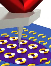 |
| Infrared laser light (purple) from below a sample (blue) excites ring-shaped nanoscale plasmonic resonator structures (gold). Hot spots (white) form in the rings' gaps. In these hot spots, infrared absorption is enhanced, allowing for more sensitive chemical recognition. A scanning AFM tip detects the expansion of the underlying material in response to absorption of infrared light.
Credit: NIST |
Abstract:
Researchers from the National Institute of Standards and Technology (NIST) and the University of Maryland have shown how to make nanoscale measurements of critical properties of plasmonic nanomaterials—the specially engineered nanostructures that modify the interaction of light and matter for a variety of applications, including sensors, cloaking (invisibility), photovoltaics and therapeutics.
New nanoscale imaging method finds application in plasmonics
Gaithersburg, MD | Posted on July 16th, 2013Their technique is one of the few that allows researchers to make actual physical measurements of these materials at the nanoscale without affecting the nanomaterial's function.
Plasmonic nanomaterials contain specially engineered conducting nanoscale structures that can enhance the interaction between light and an adjacent material, and the shape and size of such nanostructures can be adjusted to tune these interactions. Theoretical calculations are frequently used to understand and predict the optical properties of plasmonic nanomaterials, but few experimental techniques are available to study them in detail. Researchers need to be able to measure the optical properties of individual structures and how each interacts with surrounding materials directly in a way that doesn't affect how the structure functions.
"We want to maximize the sensitivity of these resonator arrays and study their properties," says lead researcher Andrea Centrone. "In order to do that, we needed an experimental technique that we could use to verify theory and to understand the influence of nanofabrication defects that are typically found in real samples. Our technique has the advantage of being extremely sensitive spatially and chemically, and the results are straightforward to interpret."
The research team turned to photothermal induced resonance (PTIR), an emerging chemically specific materials analysis technique, and showed it can be used to image the response of plasmonic nanomaterials excited by infrared (IR) light with nanometer-scale resolution.
The team used PTIR to image the absorbed energy in ring-shaped plasmonic resonators. The nanoscale resonators focus the incoming IR light within the rings' gaps to create "hot spots" where the light absorption is enhanced, which makes for more sensitive chemical identification. For the first time, the researchers precisely quantified the absorption in the hot spots and showed that for the samples under investigation, it is approximately 30 times greater than areas away from the resonators.
The researchers also showed that plasmonic materials can be used to increase the sensitivity of IR and PTIR spectroscopy for chemical analysis by enhancing the local light intensity, and thereby, the spectroscopic signal.
Their work further demonstrated the versatility of PTIR as a measurement tool that allows simultaneous measurement of a nanomaterial's shape, size, and chemical composition—the three characteristics that determine a nanomaterial's properties. Unlike many other methods for probing materials at the nanoscale, PTIR doesn't interfere with the material under investigation; it doesn't require the researcher to have prior knowledge about the material's optical properties or geometry; and it returns data that is more easily interpretable than other techniques that require separating the response of the sample from response of the probe.
*B. Lahiri, G. Holland, V. Aksyuk and A. Centrone. Nanoscale imaging of plasmonic hot spots and dark modes with the photothermal-induced resonance technique. Nano Letters. June 18, 2013. DOI: 10.1021/nl401284m.
####
For more information, please click here
Contacts:
Mark Esser
301-975-8735
Copyright © National Institute of Standards and Technology (NIST)
If you have a comment, please Contact us.Issuers of news releases, not 7th Wave, Inc. or Nanotechnology Now, are solely responsible for the accuracy of the content.
Bookmark:


| Related Links |
| Related News Press |
News and information
![]() Quantum computer improves AI predictions April 17th, 2026
Quantum computer improves AI predictions April 17th, 2026
![]() Flexible sensor gains sensitivity under pressure April 17th, 2026
Flexible sensor gains sensitivity under pressure April 17th, 2026
![]() A reusable chip for particulate matter sensing April 17th, 2026
A reusable chip for particulate matter sensing April 17th, 2026
![]() Detecting vibrational quantum beating in the predissociation dynamics of SF6 using time-resolved photoelectron spectroscopy April 17th, 2026
Detecting vibrational quantum beating in the predissociation dynamics of SF6 using time-resolved photoelectron spectroscopy April 17th, 2026
Imaging
![]() Simple algorithm paired with standard imaging tool could predict failure in lithium metal batteries August 8th, 2025
Simple algorithm paired with standard imaging tool could predict failure in lithium metal batteries August 8th, 2025
![]() First real-time observation of two-dimensional melting process: Researchers at Mainz University unveil new insights into magnetic vortex structures August 8th, 2025
First real-time observation of two-dimensional melting process: Researchers at Mainz University unveil new insights into magnetic vortex structures August 8th, 2025
![]() New imaging approach transforms study of bacterial biofilms August 8th, 2025
New imaging approach transforms study of bacterial biofilms August 8th, 2025
Laboratories
![]() Researchers develop molecular qubits that communicate at telecom frequencies October 3rd, 2025
Researchers develop molecular qubits that communicate at telecom frequencies October 3rd, 2025
Govt.-Legislation/Regulation/Funding/Policy
![]() Quantum computer improves AI predictions April 17th, 2026
Quantum computer improves AI predictions April 17th, 2026
![]() Metasurfaces smooth light to boost magnetic sensing precision January 30th, 2026
Metasurfaces smooth light to boost magnetic sensing precision January 30th, 2026
![]() New imaging approach transforms study of bacterial biofilms August 8th, 2025
New imaging approach transforms study of bacterial biofilms August 8th, 2025
Sensors
![]() Flexible sensor gains sensitivity under pressure April 17th, 2026
Flexible sensor gains sensitivity under pressure April 17th, 2026
![]() Tiny nanosheets, big leap: A new sensor detects ethanol at ultra-low levels January 30th, 2026
Tiny nanosheets, big leap: A new sensor detects ethanol at ultra-low levels January 30th, 2026
![]() From sensors to smart systems: the rise of AI-driven photonic noses January 30th, 2026
From sensors to smart systems: the rise of AI-driven photonic noses January 30th, 2026
![]() Sensors innovations for smart lithium-based batteries: advancements, opportunities, and potential challenges August 8th, 2025
Sensors innovations for smart lithium-based batteries: advancements, opportunities, and potential challenges August 8th, 2025
Discoveries
![]() Quantum computer improves AI predictions April 17th, 2026
Quantum computer improves AI predictions April 17th, 2026
![]() Flexible sensor gains sensitivity under pressure April 17th, 2026
Flexible sensor gains sensitivity under pressure April 17th, 2026
![]() A reusable chip for particulate matter sensing April 17th, 2026
A reusable chip for particulate matter sensing April 17th, 2026
![]() Detecting vibrational quantum beating in the predissociation dynamics of SF6 using time-resolved photoelectron spectroscopy April 17th, 2026
Detecting vibrational quantum beating in the predissociation dynamics of SF6 using time-resolved photoelectron spectroscopy April 17th, 2026
Announcements
![]() A fundamentally new therapeutic approach to cystic fibrosis: Nanobody repairs cellular defect April 17th, 2026
A fundamentally new therapeutic approach to cystic fibrosis: Nanobody repairs cellular defect April 17th, 2026
![]() UC Irvine physicists discover method to reverse ‘quantum scrambling’ : The work addresses the problem of information loss in quantum computing system April 17th, 2026
UC Irvine physicists discover method to reverse ‘quantum scrambling’ : The work addresses the problem of information loss in quantum computing system April 17th, 2026
Interviews/Book Reviews/Essays/Reports/Podcasts/Journals/White papers/Posters
![]() A fundamentally new therapeutic approach to cystic fibrosis: Nanobody repairs cellular defect April 17th, 2026
A fundamentally new therapeutic approach to cystic fibrosis: Nanobody repairs cellular defect April 17th, 2026
![]() UC Irvine physicists discover method to reverse ‘quantum scrambling’ : The work addresses the problem of information loss in quantum computing system April 17th, 2026
UC Irvine physicists discover method to reverse ‘quantum scrambling’ : The work addresses the problem of information loss in quantum computing system April 17th, 2026
Military
![]() Quantum engineers ‘squeeze’ laser frequency combs to make more sensitive gas sensors January 17th, 2025
Quantum engineers ‘squeeze’ laser frequency combs to make more sensitive gas sensors January 17th, 2025
![]() Chainmail-like material could be the future of armor: First 2D mechanically interlocked polymer exhibits exceptional flexibility and strength January 17th, 2025
Chainmail-like material could be the future of armor: First 2D mechanically interlocked polymer exhibits exceptional flexibility and strength January 17th, 2025
![]() Single atoms show their true color July 5th, 2024
Single atoms show their true color July 5th, 2024
![]() NRL charters Navy’s quantum inertial navigation path to reduce drift April 5th, 2024
NRL charters Navy’s quantum inertial navigation path to reduce drift April 5th, 2024
Research partnerships
![]() Lab to industry: InSe wafer-scale breakthrough for future electronics August 8th, 2025
Lab to industry: InSe wafer-scale breakthrough for future electronics August 8th, 2025
![]() HKU physicists uncover hidden order in the quantum world through deconfined quantum critical points April 25th, 2025
HKU physicists uncover hidden order in the quantum world through deconfined quantum critical points April 25th, 2025
Solar/Photovoltaic
![]() Spinel-type sulfide semiconductors to operate the next-generation LEDs and solar cells For solar-cell absorbers and green-LED source October 3rd, 2025
Spinel-type sulfide semiconductors to operate the next-generation LEDs and solar cells For solar-cell absorbers and green-LED source October 3rd, 2025
![]() KAIST researchers introduce new and improved, next-generation perovskite solar cell November 8th, 2024
KAIST researchers introduce new and improved, next-generation perovskite solar cell November 8th, 2024
![]() Groundbreaking precision in single-molecule optoelectronics August 16th, 2024
Groundbreaking precision in single-molecule optoelectronics August 16th, 2024
![]() Development of zinc oxide nanopagoda array photoelectrode: photoelectrochemical water-splitting hydrogen production January 12th, 2024
Development of zinc oxide nanopagoda array photoelectrode: photoelectrochemical water-splitting hydrogen production January 12th, 2024
|
|
||
|
|
||
| The latest news from around the world, FREE | ||
|
|
||
|
|
||
| Premium Products | ||
|
|
||
|
Only the news you want to read!
Learn More |
||
|
|
||
|
Full-service, expert consulting
Learn More |
||
|
|
||