Home > Press > Two-Dimensional Atomically-Flat Transistors Show Promise for Next Generation Green Electronics
 |
Abstract:
UC Santa Barbara researchers demonstrate first n-type field effect transistors on monolayer tungsten diselenide with record performance
Two-Dimensional Atomically-Flat Transistors Show Promise for Next Generation Green Electronics
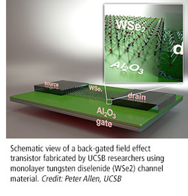
Santa Barbara, CA | Posted on June 21st, 2013Researchers at UC Santa Barbara, in collaboration with University of Notre Dame, have recently demonstrated the highest reported drive current on a transistor made of a monolayer of tungsten diselenide (WSe2), a 2-dimensional atomic crystal categorized as a transition metal dichalcogenide (TMD). The discovery is also the first demonstration of an "n-type" WSe2 field-effect-transistor (FET), showing the tremendous potential of this material for future low-power and high-performance integrated circuits.
Monolayer WSe2 is similar to graphene in that it has a hexagonal atomic structure and derives from its layered bulk form in which adjacent layers are held together by relatively weak Van der Waals forces. However, WSe2 has a key advantage over graphene.
"In addition to its atomically smooth surfaces, it has a considerable band gap of 1.6 eV," explained Kaustav Banerjee, professor of electrical and computer engineering and Director of the Nanoelectronics Research Lab at UCSB. Banerjee's research team also includes UCSB researchers Wei Liu, Jiahao Kang, Deblina Sarkar, Yasin Khatami and Professor Debdeep Jena of Notre Dame. Their study was published in the May 2013 issue of Nano Letters.
"There is growing worldwide interest in these 2D crystals due to the many possibilities they hold for the next generation of integrated electronics, optoelectronics and sensors," commented Professor Pulickel Ajayan, the Anderson Professor of Engineering at Rice University and a world renowned authority on nanomaterials. "This result is very impressive and an outcome of the detailed understanding of the physical nature of the contacts to these 2D crystals that the Santa Barbara group has developed."
"Understanding the nature of the metal-TMD interfaces was key to our successful transistor design and demonstration," explained Banerjee. Banerjee's group pioneered a methodology using ab-initio Density Functional Theory (DFT) that established the key criteria needed to evaluate such interfaces leading to the best possible contacts to the monolayer TMDs.
The DFT technique was pioneered by UCSB professor emeritus of physics Dr. Walter Kohn, for which he was awarded the Nobel Prize in Chemistry in 1998. "At a recent meeting with Professor Kohn, we discussed how this relatively new class of semiconductors is benefitting from one of his landmark contributions," said Banerjee.
Wei Liu, a post-doctoral researcher in Banerjee's group and co-author of the study, explained, "Guided by the contact evaluation methodology we have developed, our transistors achieved ON currents as high as 210 uA/um, which are the highest reported value of drive current on any monolayer TMD based FET to date." They were also able to achieve mobility of 142 cm2/V.s, which is the highest reported value for any back-gated monolayer TMD FET.
"DFT simulations provide critical insights to the various factors that effectively determine the quality of the interfaces to these 2D materials, which is necessary for achieving low contact resistances." added Jiahao Kang, a PhD student in Banerjee's group and co-author of the study.
"Nanoelectronics and energy efficient computing technology are key areas of research at UCSB, fields in which our faculty members are renowned for their achievements. With these results, Professor Banerjee's team continues to make important research contributions to next-generation electronics," commented Rod Alferness, Dean of the College of Engineering at UCSB.
Their research was supported by the National Science Foundation, the California NanoSystems Institute at UC Santa Barbara, and the Materials Research Laboratory at UCSB: an NSF MRSEC.
####
About UC Santa Barbara Engineering
The College of Engineering at University of California, Santa Barbara is recognized globally as a leader among the top tier of engineering education and research programs, and is renowned for a successful interdisciplinary approach to engineering research.
For more information, please click here
Copyright © UC Santa Barbara Engineering
If you have a comment, please Contact us.Issuers of news releases, not 7th Wave, Inc. or Nanotechnology Now, are solely responsible for the accuracy of the content.
Bookmark:


| Related News Press |
News and information
![]() Quantum computer improves AI predictions April 17th, 2026
Quantum computer improves AI predictions April 17th, 2026
![]() Flexible sensor gains sensitivity under pressure April 17th, 2026
Flexible sensor gains sensitivity under pressure April 17th, 2026
![]() A reusable chip for particulate matter sensing April 17th, 2026
A reusable chip for particulate matter sensing April 17th, 2026
![]() Detecting vibrational quantum beating in the predissociation dynamics of SF6 using time-resolved photoelectron spectroscopy April 17th, 2026
Detecting vibrational quantum beating in the predissociation dynamics of SF6 using time-resolved photoelectron spectroscopy April 17th, 2026
Graphene/ Graphite
![]() Electrifying results shed light on graphene foam as a potential material for lab grown cartilage June 6th, 2025
Electrifying results shed light on graphene foam as a potential material for lab grown cartilage June 6th, 2025
![]() Breakthrough in proton barrier films using pore-free graphene oxide: Kumamoto University researchers achieve new milestone in advanced coating technologies September 13th, 2024
Breakthrough in proton barrier films using pore-free graphene oxide: Kumamoto University researchers achieve new milestone in advanced coating technologies September 13th, 2024
Govt.-Legislation/Regulation/Funding/Policy
![]() Quantum computer improves AI predictions April 17th, 2026
Quantum computer improves AI predictions April 17th, 2026
![]() Metasurfaces smooth light to boost magnetic sensing precision January 30th, 2026
Metasurfaces smooth light to boost magnetic sensing precision January 30th, 2026
![]() New imaging approach transforms study of bacterial biofilms August 8th, 2025
New imaging approach transforms study of bacterial biofilms August 8th, 2025
Chip Technology
![]() A reusable chip for particulate matter sensing April 17th, 2026
A reusable chip for particulate matter sensing April 17th, 2026
![]() Metasurfaces smooth light to boost magnetic sensing precision January 30th, 2026
Metasurfaces smooth light to boost magnetic sensing precision January 30th, 2026
Nanoelectronics
![]() Lab to industry: InSe wafer-scale breakthrough for future electronics August 8th, 2025
Lab to industry: InSe wafer-scale breakthrough for future electronics August 8th, 2025
![]() Interdisciplinary: Rice team tackles the future of semiconductors Multiferroics could be the key to ultralow-energy computing October 6th, 2023
Interdisciplinary: Rice team tackles the future of semiconductors Multiferroics could be the key to ultralow-energy computing October 6th, 2023
![]() Key element for a scalable quantum computer: Physicists from Forschungszentrum J�lich and RWTH Aachen University demonstrate electron transport on a quantum chip September 23rd, 2022
Key element for a scalable quantum computer: Physicists from Forschungszentrum J�lich and RWTH Aachen University demonstrate electron transport on a quantum chip September 23rd, 2022
![]() Reduced power consumption in semiconductor devices September 23rd, 2022
Reduced power consumption in semiconductor devices September 23rd, 2022
Materials/Metamaterials/Magnetoresistance
![]() First real-time observation of two-dimensional melting process: Researchers at Mainz University unveil new insights into magnetic vortex structures August 8th, 2025
First real-time observation of two-dimensional melting process: Researchers at Mainz University unveil new insights into magnetic vortex structures August 8th, 2025
![]() Researchers unveil a groundbreaking clay-based solution to capture carbon dioxide and combat climate change June 6th, 2025
Researchers unveil a groundbreaking clay-based solution to capture carbon dioxide and combat climate change June 6th, 2025
![]() A 1960s idea inspires NBI researchers to study hitherto inaccessible quantum states June 6th, 2025
A 1960s idea inspires NBI researchers to study hitherto inaccessible quantum states June 6th, 2025
![]() Institute for Nanoscience hosts annual proposal planning meeting May 16th, 2025
Institute for Nanoscience hosts annual proposal planning meeting May 16th, 2025
Announcements
![]() A fundamentally new therapeutic approach to cystic fibrosis: Nanobody repairs cellular defect April 17th, 2026
A fundamentally new therapeutic approach to cystic fibrosis: Nanobody repairs cellular defect April 17th, 2026
![]() UC Irvine physicists discover method to reverse �quantum scrambling� : The work addresses the problem of information loss in quantum computing system April 17th, 2026
UC Irvine physicists discover method to reverse �quantum scrambling� : The work addresses the problem of information loss in quantum computing system April 17th, 2026
Research partnerships
![]() Lab to industry: InSe wafer-scale breakthrough for future electronics August 8th, 2025
Lab to industry: InSe wafer-scale breakthrough for future electronics August 8th, 2025
![]() HKU physicists uncover hidden order in the quantum world through deconfined quantum critical points April 25th, 2025
HKU physicists uncover hidden order in the quantum world through deconfined quantum critical points April 25th, 2025
|
|
||
|
|
||
| The latest news from around the world, FREE | ||
|
|
||
|
|
||
| Premium Products | ||
|
|
||
|
Only the news you want to read!
Learn More |
||
|
|
||
|
Full-service, expert consulting
Learn More |
||
|
|
||