Home > Press > An ultrasensitive molybdenum-based image sensor: New material can result in 5 times more sensitive cameras
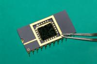 |
| This prototype is the first ever molybdenum based image sensor, 5 times more sensitive than current silicium-based technology
Credit: EPFL / Alain Herzog |
Abstract:
A new material has the potential to improve the sensitivity of photographic image sensors by a factor of five. In 2011, an EPFL team led by Andras Kis discovered the amazing semi-conducting properties of molybdenite (MoS2), and they have been exploring its potential in various technological applications ever since. This promising candidate for replacing silicon has now been integrated in a prototype of an image sensor. This sensor, described in an article appearing in Nature Nanotechnology, has five times the light sensitivity of current technology.
An ultrasensitive molybdenum-based image sensor: New material can result in 5 times more sensitive cameras
Lausanne, Switzerland | Posted on June 12th, 2013All digital cameras work according to the same principle: they convert light into an electric charge. The camera has a light sensor, whose surface is a semi-conducting material that is divided into millions of cells, or pixels. The semi-conducting material on each cell reacts to the incoming light by generating a specific electrical charge, which is then transferred to the camera's firmware for processing. The efficiency of this process depends on the quantity of light that is needed to trigger the charge transfer.
The all-time pixel record
The objective of the EPFL researchers was to demonstrate molybdenite's potential in image sensors. For this reason, their sensor only has a single pixel. But it needs five times less light to trigger a charge transfer than the silicon-based sensors that are currently available. "Our main goal is to prove that MoS2 is an ideal candidate for this kind of application," explains Kis.
This level of sensitivity would open up the huge area of low-light or night photography, without resorting to "noise"-generating amplification techniques, slowing down the shutter speed or using a flash. For some specialized domains in which light conditions are often not optimal, such as astrophotography or biological imaging, the advantage is even more obvious. "It would make it possible to take photographs using only starlight," says Kis.
A revolutionary material
Molybdenite's extraordinary properties make this performance possible. Like the silicon used in currently available sensors, molybdenite requires an electric current, which comes from the battery. To generate a pixel, the charge generated by the light energy must be greater than the threshold current from the battery.
A single-atom layer of molybdenite requires only a very small electric charge to function. Because of this, it takes much less light energy to reach the threshold needed to generate a pixel. MoS2 is a naturally abundant, inexpensive material. In addition, Kis explains, the prototype doesn't require any other semi-conductors, which should greatly simplify manufacturing processes. Kis, who is a pioneer in research on the semi-conductivity of molybdenite, recently demonstrated its potential in an integrated circuit and, in early 2013, a flash memory prototoype. With this new step into imaging, molybdenite shows its extraordinary potential in another important area of application.
####
For more information, please click here
Contacts:
Lionel Pousaz
41-795-597-161
Copyright © Ecole Polytechnique F�d�rale de Lausanne
If you have a comment, please Contact us.Issuers of news releases, not 7th Wave, Inc. or Nanotechnology Now, are solely responsible for the accuracy of the content.
Bookmark:


| Related News Press |
News and information
![]() Quantum computer improves AI predictions April 17th, 2026
Quantum computer improves AI predictions April 17th, 2026
![]() Flexible sensor gains sensitivity under pressure April 17th, 2026
Flexible sensor gains sensitivity under pressure April 17th, 2026
![]() A reusable chip for particulate matter sensing April 17th, 2026
A reusable chip for particulate matter sensing April 17th, 2026
![]() Detecting vibrational quantum beating in the predissociation dynamics of SF6 using time-resolved photoelectron spectroscopy April 17th, 2026
Detecting vibrational quantum beating in the predissociation dynamics of SF6 using time-resolved photoelectron spectroscopy April 17th, 2026
Imaging
![]() Simple algorithm paired with standard imaging tool could predict failure in lithium metal batteries August 8th, 2025
Simple algorithm paired with standard imaging tool could predict failure in lithium metal batteries August 8th, 2025
Chip Technology
![]() A reusable chip for particulate matter sensing April 17th, 2026
A reusable chip for particulate matter sensing April 17th, 2026
![]() Metasurfaces smooth light to boost magnetic sensing precision January 30th, 2026
Metasurfaces smooth light to boost magnetic sensing precision January 30th, 2026
Sensors
![]() Flexible sensor gains sensitivity under pressure April 17th, 2026
Flexible sensor gains sensitivity under pressure April 17th, 2026
![]() Tiny nanosheets, big leap: A new sensor detects ethanol at ultra-low levels January 30th, 2026
Tiny nanosheets, big leap: A new sensor detects ethanol at ultra-low levels January 30th, 2026
![]() From sensors to smart systems: the rise of AI-driven photonic noses January 30th, 2026
From sensors to smart systems: the rise of AI-driven photonic noses January 30th, 2026
![]() Sensors innovations for smart lithium-based batteries: advancements, opportunities, and potential challenges August 8th, 2025
Sensors innovations for smart lithium-based batteries: advancements, opportunities, and potential challenges August 8th, 2025
Discoveries
![]() Quantum computer improves AI predictions April 17th, 2026
Quantum computer improves AI predictions April 17th, 2026
![]() Flexible sensor gains sensitivity under pressure April 17th, 2026
Flexible sensor gains sensitivity under pressure April 17th, 2026
![]() A reusable chip for particulate matter sensing April 17th, 2026
A reusable chip for particulate matter sensing April 17th, 2026
![]() Detecting vibrational quantum beating in the predissociation dynamics of SF6 using time-resolved photoelectron spectroscopy April 17th, 2026
Detecting vibrational quantum beating in the predissociation dynamics of SF6 using time-resolved photoelectron spectroscopy April 17th, 2026
Announcements
![]() A fundamentally new therapeutic approach to cystic fibrosis: Nanobody repairs cellular defect April 17th, 2026
A fundamentally new therapeutic approach to cystic fibrosis: Nanobody repairs cellular defect April 17th, 2026
![]() UC Irvine physicists discover method to reverse �quantum scrambling� : The work addresses the problem of information loss in quantum computing system April 17th, 2026
UC Irvine physicists discover method to reverse �quantum scrambling� : The work addresses the problem of information loss in quantum computing system April 17th, 2026
|
|
||
|
|
||
| The latest news from around the world, FREE | ||
|
|
||
|
|
||
| Premium Products | ||
|
|
||
|
Only the news you want to read!
Learn More |
||
|
|
||
|
Full-service, expert consulting
Learn More |
||
|
|
||