Home > Press > Physicists find right (and left) solution for on-chip optics
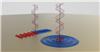 |
| Two different devices based on the herringbone pattern were presented in the Science paper: a rectangular array and a ring-shaped array (both interpreted in this illustration). Circularly polarized light with waves that wind in opposite directions gets split by both devices, with its waves routed in opposite directions. For a ring-shaped coupler, this means that plasmons are channeled either toward or away from the center of the structure. Intensity at the center of the ring can therefore be switched on and off by manipulating the polarization of the incoming light. (Image courtesy of Jiao Lin and Samuel Twist.) |
Abstract:
A Harvard-led team of researchers has created a new type of nanoscale device that converts an optical signal into waves that travel along a metal surface. Significantly, the device can recognize specific kinds of polarized light and accordingly send the signal in one direction or another.
Physicists find right (and left) solution for on-chip optics
Cambridge, MA | Posted on April 22nd, 2013The findings, published in the April 19 issue of Science, offer a new way to precisely manipulate light at the subwavelength scale without damaging a signal that could carry data. This opens the door to a new generation of on-chip optical interconnects that can efficiently funnel information from optical to electronic devices.
"If you want to send a data signal around on a tiny chip with lots of components, then you need to be able to precisely control where it's going," says co-lead author Balthasar M�ller, a graduate student at the Harvard School of Engineering and Applied Sciences (SEAS). "If you don't control it well, information will be lost. Directivity is such an important factor."
The coupler transforms incoming light into a wave called a surface plasmon polariton, a surface ripple in the sea of electrons that exists inside metals.
In the past, it has been possible to control the direction of these waves by changing the angle at which light strikes the surface of the coupler, but, as M�ller puts it, "This was a major pain. Optical circuits are very difficult to align, so readjusting the angles for the sake of routing the signal was impractical."
With the new coupler, the light simply needs to come in perpendicularly, and the device does the rest. Acting like a traffic controller, it reads the polarization of the incoming light wave�which might be linear, left-hand circular, or right-hand circular�and routes it accordingly. The device can even split apart a light beam and send parts of it in different directions, allowing for information transmission on multiple channels.
The coupler consists of a thin sheet of gold, peppered with tiny perforations. But the precise pattern of these slits, arranged rather like herringbones, is where the genius lies.
"The go-to solution until now has been a series of parallel grooves known as a grating, which does the trick but loses a large portion of the signal in the process," says principal investigator Federico Capasso, Robert L. Wallace Professor of Applied Physics and Vinton Hayes Senior Research Fellow in Electrical Engineering at Harvard SEAS. "Now perhaps the go-to solution will be our structure. It makes it possible to control the direction of signals in a very simple and elegant way."
Because the new structure is so small�each repeating unit of the pattern is smaller than the wavelength of visible light�the researchers believe it should be easy to incorporate the design into novel technologies, such as flat optics.
Yet Capasso speaks most animatedly about the possibilities for incorporating the new coupler into future high-speed information networks that may combine nanoscale electronics (which currently exist) with optical and plasmonic elements on a single microchip.
"This has generated great excitement in the field," Capasso says.
M�ller and Capasso were joined on this work by co-lead author Jiao Lin, a former SEAS postdoctoral fellow who is now at the Singapore Institute of Manufacturing Technology; and coauthors Qian Wang and Guanghui Yuan, of Nanyang Technological University, Singapore; Nicholas Antoniou, Principal FIB Engineer at the Harvard Center for Nanoscale Systems; and Xiao-Cong Yuan, a professor at the Institute of Modern Optics at Nankai University in China.
The research was supported by the U.S. Air Force Office of Scientific Research, the Agency for Science, Technology, and Research (A*STAR) in Singapore, the National Natural Science Foundation of China, the Ministry of Science and Technology of China, and the National Research Foundation of Singapore. Part of the work was performed at the Harvard Center for Nanoscale Systems, which is a member of the National Nanotechnology Infrastructure Network, supported by the U.S. National Science Foundation.
Full bibliographic information
Jiao Lin et al., "Polarization-Controlled Tunable Directional Coupling of Surface Plasmon Polaritons," SCIENCE, April 19, 2013. DOI: 10.1126/science.1233746
####
About Harvard School of Engineering and Applied Sciences
The Harvard School of Engineering and Applied Sciences (SEAS) serves as the connector and integrator of Harvard's teaching and research efforts in engineering, applied sciences, and technology.
For more information, please click here
Contacts:
Caroline Perry
617-496-1351
Copyright © Harvard School of Engineering and Applied Sciences
If you have a comment, please Contact us.Issuers of news releases, not 7th Wave, Inc. or Nanotechnology Now, are solely responsible for the accuracy of the content.
Bookmark:


| Related News Press |
News and information
![]() Quantum computer improves AI predictions April 17th, 2026
Quantum computer improves AI predictions April 17th, 2026
![]() Flexible sensor gains sensitivity under pressure April 17th, 2026
Flexible sensor gains sensitivity under pressure April 17th, 2026
![]() A reusable chip for particulate matter sensing April 17th, 2026
A reusable chip for particulate matter sensing April 17th, 2026
![]() Detecting vibrational quantum beating in the predissociation dynamics of SF6 using time-resolved photoelectron spectroscopy April 17th, 2026
Detecting vibrational quantum beating in the predissociation dynamics of SF6 using time-resolved photoelectron spectroscopy April 17th, 2026
Govt.-Legislation/Regulation/Funding/Policy
![]() Quantum computer improves AI predictions April 17th, 2026
Quantum computer improves AI predictions April 17th, 2026
![]() Metasurfaces smooth light to boost magnetic sensing precision January 30th, 2026
Metasurfaces smooth light to boost magnetic sensing precision January 30th, 2026
![]() New imaging approach transforms study of bacterial biofilms August 8th, 2025
New imaging approach transforms study of bacterial biofilms August 8th, 2025
Chip Technology
![]() A reusable chip for particulate matter sensing April 17th, 2026
A reusable chip for particulate matter sensing April 17th, 2026
![]() Metasurfaces smooth light to boost magnetic sensing precision January 30th, 2026
Metasurfaces smooth light to boost magnetic sensing precision January 30th, 2026
Optical computing/Photonic computing
![]() ICFO researchers overcome long-standing bottleneck in single photon detection with twisted 2D materials August 8th, 2025
ICFO researchers overcome long-standing bottleneck in single photon detection with twisted 2D materials August 8th, 2025
![]() Programmable electron-induced color router array May 14th, 2025
Programmable electron-induced color router array May 14th, 2025
Discoveries
![]() Quantum computer improves AI predictions April 17th, 2026
Quantum computer improves AI predictions April 17th, 2026
![]() Flexible sensor gains sensitivity under pressure April 17th, 2026
Flexible sensor gains sensitivity under pressure April 17th, 2026
![]() A reusable chip for particulate matter sensing April 17th, 2026
A reusable chip for particulate matter sensing April 17th, 2026
![]() Detecting vibrational quantum beating in the predissociation dynamics of SF6 using time-resolved photoelectron spectroscopy April 17th, 2026
Detecting vibrational quantum beating in the predissociation dynamics of SF6 using time-resolved photoelectron spectroscopy April 17th, 2026
Announcements
![]() A fundamentally new therapeutic approach to cystic fibrosis: Nanobody repairs cellular defect April 17th, 2026
A fundamentally new therapeutic approach to cystic fibrosis: Nanobody repairs cellular defect April 17th, 2026
![]() UC Irvine physicists discover method to reverse �quantum scrambling� : The work addresses the problem of information loss in quantum computing system April 17th, 2026
UC Irvine physicists discover method to reverse �quantum scrambling� : The work addresses the problem of information loss in quantum computing system April 17th, 2026
Military
![]() Quantum engineers �squeeze� laser frequency combs to make more sensitive gas sensors January 17th, 2025
Quantum engineers �squeeze� laser frequency combs to make more sensitive gas sensors January 17th, 2025
![]() Chainmail-like material could be the future of armor: First 2D mechanically interlocked polymer exhibits exceptional flexibility and strength January 17th, 2025
Chainmail-like material could be the future of armor: First 2D mechanically interlocked polymer exhibits exceptional flexibility and strength January 17th, 2025
![]() Single atoms show their true color July 5th, 2024
Single atoms show their true color July 5th, 2024
![]() NRL charters Navy�s quantum inertial navigation path to reduce drift April 5th, 2024
NRL charters Navy�s quantum inertial navigation path to reduce drift April 5th, 2024
Photonics/Optics/Lasers
![]() Metasurfaces smooth light to boost magnetic sensing precision January 30th, 2026
Metasurfaces smooth light to boost magnetic sensing precision January 30th, 2026
![]() From sensors to smart systems: the rise of AI-driven photonic noses January 30th, 2026
From sensors to smart systems: the rise of AI-driven photonic noses January 30th, 2026
Research partnerships
![]() Lab to industry: InSe wafer-scale breakthrough for future electronics August 8th, 2025
Lab to industry: InSe wafer-scale breakthrough for future electronics August 8th, 2025
![]() HKU physicists uncover hidden order in the quantum world through deconfined quantum critical points April 25th, 2025
HKU physicists uncover hidden order in the quantum world through deconfined quantum critical points April 25th, 2025
|
|
||
|
|
||
| The latest news from around the world, FREE | ||
|
|
||
|
|
||
| Premium Products | ||
|
|
||
|
Only the news you want to read!
Learn More |
||
|
|
||
|
Full-service, expert consulting
Learn More |
||
|
|
||