Home > Press > Layered '2-D nanocrystals' promising new semiconductor
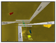 |
| Researchers are developing a new type of semiconductor technology, pictured here, for future computers and electronics based on "two-dimensional nanocrystals." The material is layered in sheets less than a nanometer thick that could replace today's silicon transistors. Birck Nanotechnology Center, Purdue University |
Abstract:
Screening and interlayer coupling in multilayer MoS2
Saptarshi Das*, 2. Joerg Appenzeller
Birck Nanotechnology Center, Purdue University
School of Electrical and Computer Engineering, Purdue University
The two-dimensional layered semiconducting di-chalcogenides are emerging as promising candidates for post-Si-CMOS applications owing to their excellent electrostatic integrity and the presence of a finite energy bandgap, unlike graphene. However, in order to unravel the ultimate potential of these materials, one needs to investigate different aspects of carrier transport. In this Letter, we present the first comprehensive experimental study on the dependence of carrier mobility on the layer thickness of back-gated multilayer MoS2 field-effect transistors. We observe a non-monotonic trend in the extracted effective field-effect mobility with layer thickness, which is of relevance for the design of high-performance devices. We also discuss a detailed theoretical model based on Thomas-Fermi charge screening and interlayer coupling in order to explain our experimental observations. Our model is generic and, therefore, is believed to be applicable to any two-dimensional layered system.
Layered '2-D nanocrystals' promising new semiconductor
West Lafayette, IN | Posted on April 15th, 2013Researchers are developing a new type of semiconductor technology for future computers and electronics based on "two-dimensional nanocrystals" layered in sheets less than a nanometer thick that could replace today's transistors.
The layered structure is made of a material called molybdenum disulfide, which belongs to a new class of semiconductors - metal di-chalogenides - emerging as potential candidates to replace today's technology, complementary metal oxide semiconductors, or CMOS.
New technologies will be needed to allow the semiconductor industry to continue advances in computer performance driven by the ability to create ever-smaller transistors. It is becoming increasingly difficult, however, to continue shrinking electronic devices made of conventional silicon-based semiconductors.
"We are going to reach the fundamental limits of silicon-based CMOS technology very soon, and that means novel materials must be found in order to continue scaling," said Saptarshi Das, who has completed a doctoral degree, working with Joerg Appenzeller, a professor of electrical and computer engineering and scientific director of nanoelectronics at Purdue's Birck Nanotechnology Center. "I don't think silicon can be replaced by a single material, but probably different materials will co-exist in a hybrid technology."
The nanocrystals are called two-dimensional because the materials can exist in the form of extremely thin sheets with a thickness of 0.7 nanometers, or roughly the width of three or four atoms. Findings show that the material performs best when formed into sheets of about 15 layers with a total thickness of 8-12 nanometers. The researchers also have developed a model to explain these experimental observations.
Findings are appearing this month as a cover story in the journal Rapid Research Letters. The paper was co-authored by Das and Appenzeller, who also have co-authored a paper to be presented during the annual Device Research Conference at the University of Notre Dame from June 23-26.
"Our model is generic and, therefore, is believed to be applicable to any two-dimensional layered system," Das said.
Molybdenum disulfide is promising in part because it possesses a bandgap, a trait that is needed to switch on and off, which is critical for digital transistors to store information in binary code.
Analyzing the material or integrating it into a circuit requires a metal contact. However, one factor limiting the ability to measure the electrical properties of a semiconductor is the electrical resistance in the contact. The researchers eliminated this contact resistance using a metal called scandium, allowing them to determine the true electronic properties of the layered device. Their results have been published in the January issue of the journal Nano Letters with doctoral students Hong-Yan Chen and Ashish Verma Penumatcha as the other co-authors.
Transistors contain critical components called gates, which enable the devices to switch on and off and to direct the flow of electrical current. In today's chips, the length of these gates is about 14 nanometers, or billionths of a meter.
The semiconductor industry plans to reduce the gate length to 6 nanometers by 2020. However, further size reductions and boosts in speed are likely not possible using silicon, meaning new designs and materials will be needed to continue progress.
####
For more information, please click here
Contacts:
Writer:
Emil Venere
765-494-4709
Sources:
Saptarshi Das
Joerg Appenzeller
765 494-1076
Copyright © Purdue University
If you have a comment, please Contact us.Issuers of news releases, not 7th Wave, Inc. or Nanotechnology Now, are solely responsible for the accuracy of the content.
Bookmark:


| Related Links |
![]() Network for Computational Nanotechnology:
Network for Computational Nanotechnology:
| Related News Press |
News and information
![]() Quantum computer improves AI predictions April 17th, 2026
Quantum computer improves AI predictions April 17th, 2026
![]() Flexible sensor gains sensitivity under pressure April 17th, 2026
Flexible sensor gains sensitivity under pressure April 17th, 2026
![]() A reusable chip for particulate matter sensing April 17th, 2026
A reusable chip for particulate matter sensing April 17th, 2026
![]() Detecting vibrational quantum beating in the predissociation dynamics of SF6 using time-resolved photoelectron spectroscopy April 17th, 2026
Detecting vibrational quantum beating in the predissociation dynamics of SF6 using time-resolved photoelectron spectroscopy April 17th, 2026
Possible Futures
![]() A fundamentally new therapeutic approach to cystic fibrosis: Nanobody repairs cellular defect April 17th, 2026
A fundamentally new therapeutic approach to cystic fibrosis: Nanobody repairs cellular defect April 17th, 2026
![]() UC Irvine physicists discover method to reverse �quantum scrambling� : The work addresses the problem of information loss in quantum computing system April 17th, 2026
UC Irvine physicists discover method to reverse �quantum scrambling� : The work addresses the problem of information loss in quantum computing system April 17th, 2026
Chip Technology
![]() A reusable chip for particulate matter sensing April 17th, 2026
A reusable chip for particulate matter sensing April 17th, 2026
![]() Metasurfaces smooth light to boost magnetic sensing precision January 30th, 2026
Metasurfaces smooth light to boost magnetic sensing precision January 30th, 2026
Nanoelectronics
![]() Lab to industry: InSe wafer-scale breakthrough for future electronics August 8th, 2025
Lab to industry: InSe wafer-scale breakthrough for future electronics August 8th, 2025
![]() Interdisciplinary: Rice team tackles the future of semiconductors Multiferroics could be the key to ultralow-energy computing October 6th, 2023
Interdisciplinary: Rice team tackles the future of semiconductors Multiferroics could be the key to ultralow-energy computing October 6th, 2023
![]() Key element for a scalable quantum computer: Physicists from Forschungszentrum J�lich and RWTH Aachen University demonstrate electron transport on a quantum chip September 23rd, 2022
Key element for a scalable quantum computer: Physicists from Forschungszentrum J�lich and RWTH Aachen University demonstrate electron transport on a quantum chip September 23rd, 2022
![]() Reduced power consumption in semiconductor devices September 23rd, 2022
Reduced power consumption in semiconductor devices September 23rd, 2022
Discoveries
![]() Quantum computer improves AI predictions April 17th, 2026
Quantum computer improves AI predictions April 17th, 2026
![]() Flexible sensor gains sensitivity under pressure April 17th, 2026
Flexible sensor gains sensitivity under pressure April 17th, 2026
![]() A reusable chip for particulate matter sensing April 17th, 2026
A reusable chip for particulate matter sensing April 17th, 2026
![]() Detecting vibrational quantum beating in the predissociation dynamics of SF6 using time-resolved photoelectron spectroscopy April 17th, 2026
Detecting vibrational quantum beating in the predissociation dynamics of SF6 using time-resolved photoelectron spectroscopy April 17th, 2026
Announcements
![]() A fundamentally new therapeutic approach to cystic fibrosis: Nanobody repairs cellular defect April 17th, 2026
A fundamentally new therapeutic approach to cystic fibrosis: Nanobody repairs cellular defect April 17th, 2026
![]() UC Irvine physicists discover method to reverse �quantum scrambling� : The work addresses the problem of information loss in quantum computing system April 17th, 2026
UC Irvine physicists discover method to reverse �quantum scrambling� : The work addresses the problem of information loss in quantum computing system April 17th, 2026
|
|
||
|
|
||
| The latest news from around the world, FREE | ||
|
|
||
|
|
||
| Premium Products | ||
|
|
||
|
Only the news you want to read!
Learn More |
||
|
|
||
|
Full-service, expert consulting
Learn More |
||
|
|
||