Home > Press > Diamond as a Building Material for Optical Circuits: A Revolution in Optomechanical Materials Enables Manufacturing of Monolithic Components / Easy Industrial Processing of Robust Polycrystalline Diamonds / Precision Sensors for Oscillation Measurement
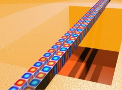 |
| Two parallel free-standing waveguides made of polycrystalline diamond serve as mechanical resonators. Optical fields (red/blue) are observed to propagate inside of them. Graphic: KIT/CFN/Pernice |
Abstract:
The application of light for information processing opens up a multitude of possibilities. However, to be able to adequately use photons in circuits and sensors, materials need to have particular optical and mechanical properties. Researchers at the Karlsruhe Institute of Technology (KIT) have now for the first time used polycrystalline diamond to manufacture optical circuits and have published their results online in Nature Communications (DOI: 10.1038/ncomms2710).
Diamond as a Building Material for Optical Circuits: A Revolution in Optomechanical Materials Enables Manufacturing of Monolithic Components / Easy Industrial Processing of Robust Polycrystalline Diamonds / Precision Sensors for Oscillation Measurement
Karlsruhe, Germany | Posted on April 11th, 2013"Diamond has several properties that allow us to manufacture all components of a ready-to-use optomechanical circuit monolithically, so to speak," says KIT research group leader Wolfram Pernice. "The elements thus manufactured that is, the resonators, circuits, and the wafer, are attractive because of their high quality."
Diamond is optically transparent to light waves of a wide range of wavelengths including the visible spectrum between 400 and 750 nm. It is due to this fact that it can be used specifically in optomechanical circuits for applications in sensor technology and fluorescence imaging, or for novel optical biological measuring methods. Whereas the high refractive index of diamond and the absence of absorption allow an efficient photon transport, its high modulus of elasticity makes it a robust material which adapts excellently to rough surfaces and releases heat rapidly.
So far, optical circuits have been manufactured using monocrystalline diamond substrates i.e., highly pure crystals with typically no more than one impurity atom to every one billion diamond atoms. Such circuits are bound to be small and their application to optical systems has required sophisticated fabrication methods.
Now, for the first time, the research group headed by Pernice used polycrystalline diamond for the fabrication of wafer-based optomechanical circuits. Even though its crystal structures are more irregular, polycrystalline diamond is robust and thus can be more easily processed. It is due to these specific properties that polycrystalline diamond can be used on much larger areas than monocrystalline material. Polycrystalline diamond conducts photons almost as efficiently as the monocrystalline substrate and is suitable for industrial use. As a matter of fact, monolithic optomechanical components could not have been manufactured without this new material.
Optomechanics combines integrated optics with mechanical elements e.g., with nanomechanical resonators in the case of the optomechanical circuit developed by Pernice and his group. These oscillatory systems react to a certain frequency. When that frequency occurs, the resonator is excited into vibration. "Nanomechanical resonators are among today's most sensitive sensors and are used in various precision measurements. It is extremely difficult, however, to address such smallest components through conventional measuring methods," explains Patrik Rath, first author of the study. "In our study, we have made use of the fact that today, nanophotonic components can be manufactured in the same sizes as nanoscale mechanical resonators. When the resonator responds, corresponding optical signals are transferred directly to the circuit." This novel development has allowed the combining of once separate fields of research and has enabled the realization of highly efficient optomechanical circuits.
Integrated optics works in a similar manner to integrated electrical circuits. Whereas optical circuits transmit information via photons, conventional electronic circuits transfer data via electrons. Integrated optics aims to combine all components required for optical communication in an integrated optical circuit to avoid a detour via electrical signals. In both cases, the respective circuits are applied to slices less than one mm in thickness i.e., to the so-called wafers.
The polycrystalline diamond was manufactured in cooperation with the Fraunhofer Institute for Applied Solid State Physics and the company Diamond Materials in Freiburg, Germany. The prototypes manufactured within the Integrated Quantum Photonics-project at the DFG Center for Functional Nanostructures (CFN) in Karlsruhe open up new ways for entirely optically controlled platforms that are increasingly needed in fundamental research and advanced sensor technologies. These technologies include accelerometers that are integrated in various electronic devices such as airbag sensors or smartphone waterlevels.
####
About Helmholtz Association of German Research Centres
The Helmholtz Association is dedicated to pursuing the long-term research goals of state and society, and to maintaining and improving the livelihoods of the population. In order to do this, the Helmholtz Association carries out top-level research to identify and explore the major challenges facing society, science and the economy. Its work is divided into six strategic research fields: Energy; Earth and Environment; Health; Key Technologies; Structure of Matter; and Aeronautics, Space and Transport. The Helmholtz Association brings together 18 scientific-technical and biological-medical research centres. With some 32,698 employees and an annual budget of approximately �3.4 billion, the Helmholtz Association is Germany�s largest scientific organisation. Its work follows in the tradition of the great natural scientist Hermann von Helmholtz (1821-1894).
About The DFG Center of Functional Nanostructures (CFN)
The DFG Center of Functional Nanostructures (CFN) devotes its attention to the important area of nanotechnology and functional nanostructures. Its objective is to carry out excellent interdisciplinary and international research in order to produce nanostructures with new technical functions and take the first step from fundamental research to application. At the present time, more than 250 scientists and engineers cooperate in more than 80 sub-projects networked through the CFN in Karlsruhe, focusing on the areas of nano-photonics, nano-electronics, molecular nanostructures, nano-biology, and nano-energy. www.cfn.kit.edu
About Karlsruhe Institute of Technology (KIT)
Karlsruhe Institute of Technology (KIT) is a public corporation according to the legislation of the state of Baden-W�rttemberg. It fulfills the mission of a university and the mission of a national research center of the Helmholtz Association. KIT focuses on a knowledge triangle that links the tasks of research, teaching, and innovation.
For more information, please click here
Contacts:
Monika Landgraf
49-721-608-47414
Fax: +49 721 608-43658
Tatjana Erkert
DFG-Centrum f�r Funktionelle Nanostrukturen (CFN)
Tel.: +49 721 608-43409
Fax: +49 721 608-48496
tatjana erkert∂kit edu
Copyright © Helmholtz Association of German Research Centres
If you have a comment, please Contact us.Issuers of news releases, not 7th Wave, Inc. or Nanotechnology Now, are solely responsible for the accuracy of the content.
Bookmark:


| Related Links |
![]() The study is available on the portal of Nature:
The study is available on the portal of Nature:
| Related News Press |
News and information
![]() Quantum computer improves AI predictions April 17th, 2026
Quantum computer improves AI predictions April 17th, 2026
![]() Flexible sensor gains sensitivity under pressure April 17th, 2026
Flexible sensor gains sensitivity under pressure April 17th, 2026
![]() A reusable chip for particulate matter sensing April 17th, 2026
A reusable chip for particulate matter sensing April 17th, 2026
![]() Detecting vibrational quantum beating in the predissociation dynamics of SF6 using time-resolved photoelectron spectroscopy April 17th, 2026
Detecting vibrational quantum beating in the predissociation dynamics of SF6 using time-resolved photoelectron spectroscopy April 17th, 2026
Laboratories
![]() Researchers develop molecular qubits that communicate at telecom frequencies October 3rd, 2025
Researchers develop molecular qubits that communicate at telecom frequencies October 3rd, 2025
![]() A battery�s hopping ions remember where they�ve been: Seen in atomic detail, the seemingly smooth flow of ions through a battery�s electrolyte is surprisingly complicated February 16th, 2024
A battery�s hopping ions remember where they�ve been: Seen in atomic detail, the seemingly smooth flow of ions through a battery�s electrolyte is surprisingly complicated February 16th, 2024
Govt.-Legislation/Regulation/Funding/Policy
![]() Quantum computer improves AI predictions April 17th, 2026
Quantum computer improves AI predictions April 17th, 2026
![]() Metasurfaces smooth light to boost magnetic sensing precision January 30th, 2026
Metasurfaces smooth light to boost magnetic sensing precision January 30th, 2026
![]() New imaging approach transforms study of bacterial biofilms August 8th, 2025
New imaging approach transforms study of bacterial biofilms August 8th, 2025
Chip Technology
![]() A reusable chip for particulate matter sensing April 17th, 2026
A reusable chip for particulate matter sensing April 17th, 2026
![]() Metasurfaces smooth light to boost magnetic sensing precision January 30th, 2026
Metasurfaces smooth light to boost magnetic sensing precision January 30th, 2026
Optical computing/Photonic computing
![]() ICFO researchers overcome long-standing bottleneck in single photon detection with twisted 2D materials August 8th, 2025
ICFO researchers overcome long-standing bottleneck in single photon detection with twisted 2D materials August 8th, 2025
![]() Programmable electron-induced color router array May 14th, 2025
Programmable electron-induced color router array May 14th, 2025
Sensors
![]() Flexible sensor gains sensitivity under pressure April 17th, 2026
Flexible sensor gains sensitivity under pressure April 17th, 2026
![]() Tiny nanosheets, big leap: A new sensor detects ethanol at ultra-low levels January 30th, 2026
Tiny nanosheets, big leap: A new sensor detects ethanol at ultra-low levels January 30th, 2026
![]() From sensors to smart systems: the rise of AI-driven photonic noses January 30th, 2026
From sensors to smart systems: the rise of AI-driven photonic noses January 30th, 2026
![]() Sensors innovations for smart lithium-based batteries: advancements, opportunities, and potential challenges August 8th, 2025
Sensors innovations for smart lithium-based batteries: advancements, opportunities, and potential challenges August 8th, 2025
Discoveries
![]() Quantum computer improves AI predictions April 17th, 2026
Quantum computer improves AI predictions April 17th, 2026
![]() Flexible sensor gains sensitivity under pressure April 17th, 2026
Flexible sensor gains sensitivity under pressure April 17th, 2026
![]() A reusable chip for particulate matter sensing April 17th, 2026
A reusable chip for particulate matter sensing April 17th, 2026
![]() Detecting vibrational quantum beating in the predissociation dynamics of SF6 using time-resolved photoelectron spectroscopy April 17th, 2026
Detecting vibrational quantum beating in the predissociation dynamics of SF6 using time-resolved photoelectron spectroscopy April 17th, 2026
Announcements
![]() A fundamentally new therapeutic approach to cystic fibrosis: Nanobody repairs cellular defect April 17th, 2026
A fundamentally new therapeutic approach to cystic fibrosis: Nanobody repairs cellular defect April 17th, 2026
![]() UC Irvine physicists discover method to reverse �quantum scrambling� : The work addresses the problem of information loss in quantum computing system April 17th, 2026
UC Irvine physicists discover method to reverse �quantum scrambling� : The work addresses the problem of information loss in quantum computing system April 17th, 2026
Photonics/Optics/Lasers
![]() Metasurfaces smooth light to boost magnetic sensing precision January 30th, 2026
Metasurfaces smooth light to boost magnetic sensing precision January 30th, 2026
![]() From sensors to smart systems: the rise of AI-driven photonic noses January 30th, 2026
From sensors to smart systems: the rise of AI-driven photonic noses January 30th, 2026
|
|
||
|
|
||
| The latest news from around the world, FREE | ||
|
|
||
|
|
||
| Premium Products | ||
|
|
||
|
Only the news you want to read!
Learn More |
||
|
|
||
|
Full-service, expert consulting
Learn More |
||
|
|
||