Home > Press > New 2D material for next generation high-speed electronics
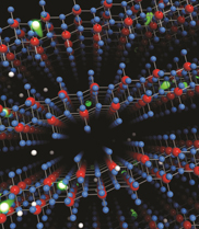 |
| Artist impression of high carrier mobility through layered molybdenum oxide crystal lattice. Credit: Dr Daniel J White, ScienceFX |
Abstract:
Scientists at CSIRO and RMIT University have produced a new two-dimensional material that could revolutionise the electronics market, making "nano" more than just a marketing term.
New 2D material for next generation high-speed electronics
Clayton, Australia | Posted on January 22nd, 2013The material - made up of layers of crystal known as molybdenum oxides - has unique properties that encourage the free flow of electrons at ultra-high speeds.
In a paper published in the January issue of materials science journal Advanced Materials, the researchers explain how they adapted a revolutionary material known as graphene to create a new conductive nano-material.
Graphene was created in 2004 by scientists in the UK and won its inventors a Nobel Prize in 2010. While graphene supports high speed electrons, its physical properties prevent it from being used for high-speed electronics.
The CSIRO's Dr Serge Zhuiykov said the new nano-material was made up of layered sheets - similar to graphite layers that make up a pencil's core.
"Within these layers, electrons are able to zip through at high speeds with minimal scattering," Dr Zhuiykov said.
"The importance of our breakthrough is how quickly and fluently electrons - which conduct electricity - are able to flow through the new material."
RMIT's Professor Kourosh Kalantar-zadeh said the researchers were able to remove "road blocks" that could obstruct the electrons, an essential step for the development of high-speed electronics.
"Instead of scattering when they hit road blocks, as they would in conventional materials, they can simply pass through this new material and get through the structure faster," Professor Kalantar-zadeh said.
"Quite simply, if electrons can pass through a structure quicker, we can build devices that are smaller and transfer data at much higher speeds.
"While more work needs to be done before we can develop actual gadgets using this new 2D nano-material, this breakthrough lays the foundation for a new electronics revolution and we look forward to exploring its potential."
In the paper titled 'Enhanced Charge Carrier Mobility in Two-Dimensional High Dielectric Molybdenum Oxide,' the researchers describe how they used a process known as "exfoliation" to create layers of the material ~11 nm thick.
The material was manipulated to convert it into a semiconductor and nanoscale transistors were then created using molybdenum oxide.
The result was electron mobility values of >1,100 cm2/Vs - exceeding the current industry standard for low dimensional silicon.
The work, with RMIT doctoral researcher Sivacarendran Balendhran as the lead author, was supported by the CSIRO Sensors and Sensor Networks Transformational Capability Platform and the CSIRO Materials Science and Engineering Division.
It was also a result of collaboration between researchers from Monash University, University of California - Los Angeles (UCLA), CSIRO, Massachusetts Institute of Technology (MIT) and RMIT.
####
For more information, please click here
Contacts:
Simon Hunter
61-395-458-412
Copyright © CSIRO Australia
If you have a comment, please Contact us.Issuers of news releases, not 7th Wave, Inc. or Nanotechnology Now, are solely responsible for the accuracy of the content.
Bookmark:


| Related News Press |
News and information
![]() Quantum computer improves AI predictions April 17th, 2026
Quantum computer improves AI predictions April 17th, 2026
![]() Flexible sensor gains sensitivity under pressure April 17th, 2026
Flexible sensor gains sensitivity under pressure April 17th, 2026
![]() A reusable chip for particulate matter sensing April 17th, 2026
A reusable chip for particulate matter sensing April 17th, 2026
![]() Detecting vibrational quantum beating in the predissociation dynamics of SF6 using time-resolved photoelectron spectroscopy April 17th, 2026
Detecting vibrational quantum beating in the predissociation dynamics of SF6 using time-resolved photoelectron spectroscopy April 17th, 2026
Chip Technology
![]() A reusable chip for particulate matter sensing April 17th, 2026
A reusable chip for particulate matter sensing April 17th, 2026
![]() Metasurfaces smooth light to boost magnetic sensing precision January 30th, 2026
Metasurfaces smooth light to boost magnetic sensing precision January 30th, 2026
Nanoelectronics
![]() Lab to industry: InSe wafer-scale breakthrough for future electronics August 8th, 2025
Lab to industry: InSe wafer-scale breakthrough for future electronics August 8th, 2025
![]() Interdisciplinary: Rice team tackles the future of semiconductors Multiferroics could be the key to ultralow-energy computing October 6th, 2023
Interdisciplinary: Rice team tackles the future of semiconductors Multiferroics could be the key to ultralow-energy computing October 6th, 2023
![]() Key element for a scalable quantum computer: Physicists from Forschungszentrum J�lich and RWTH Aachen University demonstrate electron transport on a quantum chip September 23rd, 2022
Key element for a scalable quantum computer: Physicists from Forschungszentrum J�lich and RWTH Aachen University demonstrate electron transport on a quantum chip September 23rd, 2022
![]() Reduced power consumption in semiconductor devices September 23rd, 2022
Reduced power consumption in semiconductor devices September 23rd, 2022
Discoveries
![]() Quantum computer improves AI predictions April 17th, 2026
Quantum computer improves AI predictions April 17th, 2026
![]() Flexible sensor gains sensitivity under pressure April 17th, 2026
Flexible sensor gains sensitivity under pressure April 17th, 2026
![]() A reusable chip for particulate matter sensing April 17th, 2026
A reusable chip for particulate matter sensing April 17th, 2026
![]() Detecting vibrational quantum beating in the predissociation dynamics of SF6 using time-resolved photoelectron spectroscopy April 17th, 2026
Detecting vibrational quantum beating in the predissociation dynamics of SF6 using time-resolved photoelectron spectroscopy April 17th, 2026
Announcements
![]() A fundamentally new therapeutic approach to cystic fibrosis: Nanobody repairs cellular defect April 17th, 2026
A fundamentally new therapeutic approach to cystic fibrosis: Nanobody repairs cellular defect April 17th, 2026
![]() UC Irvine physicists discover method to reverse �quantum scrambling� : The work addresses the problem of information loss in quantum computing system April 17th, 2026
UC Irvine physicists discover method to reverse �quantum scrambling� : The work addresses the problem of information loss in quantum computing system April 17th, 2026
Research partnerships
![]() Lab to industry: InSe wafer-scale breakthrough for future electronics August 8th, 2025
Lab to industry: InSe wafer-scale breakthrough for future electronics August 8th, 2025
![]() HKU physicists uncover hidden order in the quantum world through deconfined quantum critical points April 25th, 2025
HKU physicists uncover hidden order in the quantum world through deconfined quantum critical points April 25th, 2025
|
|
||
|
|
||
| The latest news from around the world, FREE | ||
|
|
||
|
|
||
| Premium Products | ||
|
|
||
|
Only the news you want to read!
Learn More |
||
|
|
||
|
Full-service, expert consulting
Learn More |
||
|
|
||