Home > Press > Advanced Materials Physics: A transparent view at UC Berkeley
 |
Abstract:
Researchers have developed a transparent diode with copper-alloyed zinc sulfide as p-type conducting material.
Advanced Materials Physics: A transparent view at UC Berkeley
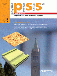
Germany | Posted on December 7th, 2012The most recent issue of physica status solidi - pss (a) presents on the cover a photograph of a tower building being familiar to many scholars and researchers in the US and beyond. It shows the famous landmark of the Berkeley campus named Sather Tower, the Campanile of the University of California. If you are now wondering why the picture looks slightly fuzzy and faint, this is not owing to hot air on a sunny day, limited talent of the photographer or low performance of his equipment. On the contrary - the image is a proof of particularly high quality, namely that of the transparent semiconductor device through which it has been taken. The somewhat darker rectangular shadow surrounding the tower are the edges of a p-CuZnS/n-ZnO diode which has been recently prepared and developed by the groups of Ramamoorth Ramesh and Joel Ager of UC Berkeley and Lawrence Berkeley National Laboratory. It is schematically depicted on the lower left side of the cover picture.
Transparent conductors are essential components of modern electronics, ranging from solar cells over light emitting diodes to flat-panel displays. Researchers are intensely searching for alternatives to the traditionally used indium tin oxide (ITO) whose costs are rising due to scarcity and increasing demand for indium. Among oxides, ZnO is a candidate which, however, like most of these materials usually exhibits only n-type conductivity, making it difficult to produce bipolar devices like diodes or thin-film transistors. The authors of the pss (a) article, Anthony M. Diamond et al., have now assessed ZnS for this purpose which so far had been mainly known as a phosphor material. They were able to produce a p-type film with 10% Cu content which, at a thickness of 200 nm, still exhibits an optical transmission of 65% at a light wavelength of 550 nm. The highest conductivity (54 S cm-1) found is also comparable to the best reported other p-type materials, but with the advantage of elements zinc, sulfur and copper being abundant. These favorable properties have allowed them to produce a transparent heterojunction diode from the two components CuZnS and ZnO. After further optimization, this should allow application of this materials system for a variety of new transparent devices.
The article is the latest highlight in the new �Advanced Materials Physics' category launched earlier this year in pss (a). Selected articles feature outstanding work at the forefront and interface between solid state physics and materials science. A recent set of further free-to-read examples covers topics such as magnetoelectrics, nanophotonics and ionic conduction.
####
For more information, please click here
Copyright © Wiley-VCH Materials Science Journals
If you have a comment, please Contact us.Issuers of news releases, not 7th Wave, Inc. or Nanotechnology Now, are solely responsible for the accuracy of the content.
Bookmark:


| Related Links |
![]() Link to the original paper on Wiley Online Library:
Link to the original paper on Wiley Online Library:
| Related News Press |
News and information
![]() Quantum computer improves AI predictions April 17th, 2026
Quantum computer improves AI predictions April 17th, 2026
![]() Flexible sensor gains sensitivity under pressure April 17th, 2026
Flexible sensor gains sensitivity under pressure April 17th, 2026
![]() A reusable chip for particulate matter sensing April 17th, 2026
A reusable chip for particulate matter sensing April 17th, 2026
![]() Detecting vibrational quantum beating in the predissociation dynamics of SF6 using time-resolved photoelectron spectroscopy April 17th, 2026
Detecting vibrational quantum beating in the predissociation dynamics of SF6 using time-resolved photoelectron spectroscopy April 17th, 2026
Chip Technology
![]() A reusable chip for particulate matter sensing April 17th, 2026
A reusable chip for particulate matter sensing April 17th, 2026
![]() Metasurfaces smooth light to boost magnetic sensing precision January 30th, 2026
Metasurfaces smooth light to boost magnetic sensing precision January 30th, 2026
Discoveries
![]() Quantum computer improves AI predictions April 17th, 2026
Quantum computer improves AI predictions April 17th, 2026
![]() Flexible sensor gains sensitivity under pressure April 17th, 2026
Flexible sensor gains sensitivity under pressure April 17th, 2026
![]() A reusable chip for particulate matter sensing April 17th, 2026
A reusable chip for particulate matter sensing April 17th, 2026
![]() Detecting vibrational quantum beating in the predissociation dynamics of SF6 using time-resolved photoelectron spectroscopy April 17th, 2026
Detecting vibrational quantum beating in the predissociation dynamics of SF6 using time-resolved photoelectron spectroscopy April 17th, 2026
Announcements
![]() A fundamentally new therapeutic approach to cystic fibrosis: Nanobody repairs cellular defect April 17th, 2026
A fundamentally new therapeutic approach to cystic fibrosis: Nanobody repairs cellular defect April 17th, 2026
![]() UC Irvine physicists discover method to reverse �quantum scrambling� : The work addresses the problem of information loss in quantum computing system April 17th, 2026
UC Irvine physicists discover method to reverse �quantum scrambling� : The work addresses the problem of information loss in quantum computing system April 17th, 2026
Interviews/Book Reviews/Essays/Reports/Podcasts/Journals/White papers/Posters
![]() A fundamentally new therapeutic approach to cystic fibrosis: Nanobody repairs cellular defect April 17th, 2026
A fundamentally new therapeutic approach to cystic fibrosis: Nanobody repairs cellular defect April 17th, 2026
![]() UC Irvine physicists discover method to reverse �quantum scrambling� : The work addresses the problem of information loss in quantum computing system April 17th, 2026
UC Irvine physicists discover method to reverse �quantum scrambling� : The work addresses the problem of information loss in quantum computing system April 17th, 2026
|
|
||
|
|
||
| The latest news from around the world, FREE | ||
|
|
||
|
|
||
| Premium Products | ||
|
|
||
|
Only the news you want to read!
Learn More |
||
|
|
||
|
Full-service, expert consulting
Learn More |
||
|
|
||