Home > Press > New method monitors semiconductor etching as it happens – with light
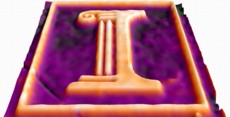 |
| Photo by Chris Edwards, Amir Arbabi, Gabriel Popescu, and Lynford Goddard
A three-dimensional image of an etched gallium-arsenide semiconductor, taken during etching with a new microscopy technique that monitors the etching process on the nanometer scale. The height difference between the orange and purple regions is approximately 250 nanometers. |
Abstract:
University of Illinois researchers have a new low-cost method to carve delicate features onto semiconductor wafers using light - and watch as it happens.
New method monitors semiconductor etching as it happens – with light
Champaign, IL | Posted on September 29th, 2012"You can use light to image the topography and you can use light to sculpture the topography," said electrical and computer engineering professor Gabriel Popescu. "It could change the future of semiconductor etching."
Chip makers and semiconductor researchers need to very precisely control the dimensions of their devices. The dimensions of the components affect performance, speed, error rate and time to failure.
Semiconductors are commonly shaped by etching with chemicals. Etching errors, such as residual layers, can affect the ability to further process and etch as well as hamper device performance. Thus, researchers use time-consuming and costly processes to ensure precise etching - for some applications, to within a scant few nanometers.
The Illinois researchers' new technique can monitor a semiconductor's surface as it is etched, in real time, with nanometer resolution. It uses a special type of microscope that uses two beams of light to very precisely measure topography.
"The idea is that the height of the structure can be determined as the light reflects off the different surfaces," said electrical and computer engineering professor Lynford Goddard, who co-led the group with Popescu. "Looking at the change in height, you figure out the etch rate. What this allows us to do is monitor it while it's etching. It allows us to figure out the etch rate both across time and across space, because we can determine the rate at every location within the semiconductor wafer that's in our field of view."
The new method is faster, lower in cost, and less noisy than the widely used methods of atomic force microscopy or scanning tunneling microscopy, which cannot monitor etching in progress but only compare before and after measurements. In addition, the new method is purely optical, so there's no contact with the semiconductor surface and the researchers can monitor the whole wafer at once instead of point-by-point.
"I would say the main advantage of our optical technique is that it requires no contact," Popescu said. "We're just sending light, reflected off the sample, as opposed to an AFM where you need to come with a probe close to the sample."
In addition to monitoring the etching process, the light catalyzes the etching process itself, called photochemical etching. Traditional chemical etching creates features in steps or plateaus. For curved surfaces or other shapes, semiconductor researchers use photochemical etching. Usually, light shines though very expensive glass plates called masks that have distinct patterns of gray to let light through by degrees. A researcher must purchase or make a mask for each tweak of a pattern until the correct pattern of features is achieved.
By contrast, the new method uses a projector to shine a grayscale image onto the sample being etched. This allows the researchers to create complex patterns quickly and easily, and adjust them as needed.
"To create each mask is very expensive. That's impractical for research," Goddard said. "Because our technique is controlled by the computer, it can be dynamic. So you can start off etching one particular shape, midway through realize that you want to make some change, and then change the projector pattern to get the desired outcome."
The researchers envision this technology applied beyond etching, to real-time monitoring of other processes in materials science and life science - for example, watching carbon nanotubes self-assemble, or error monitoring during large-scale computer chip manufacturing. It could help chip manufacturers reduce costs and processing time by ensuring that equipment stays calibrated.
The National Science Foundation supported this work, published Sept. 28 in the journal Light: Science and Applications. Goddard and Popescu are also affiliated with the Beckman Institute for Advanced Science and Technology at the U. of I.
Graduate students Chris Edwards and Amir Arbabi were also co-authors of the paper.
####
For more information, please click here
Contacts:
Liz Ahlberg
Physical Sciences Editor
217-244-1073
Lynford Goddard
217-244-0799
To reach
Gabriel Popescu
217-333-4840
Copyright © University of Illinois at Urbana-Champaign
If you have a comment, please Contact us.Issuers of news releases, not 7th Wave, Inc. or Nanotechnology Now, are solely responsible for the accuracy of the content.
Bookmark:


| Related Links |
![]() Beckman Institute for Advanced Science and Technology at the U. of I.:
Beckman Institute for Advanced Science and Technology at the U. of I.:
| Related News Press |
News and information
![]() Quantum computer improves AI predictions April 17th, 2026
Quantum computer improves AI predictions April 17th, 2026
![]() Flexible sensor gains sensitivity under pressure April 17th, 2026
Flexible sensor gains sensitivity under pressure April 17th, 2026
![]() A reusable chip for particulate matter sensing April 17th, 2026
A reusable chip for particulate matter sensing April 17th, 2026
![]() Detecting vibrational quantum beating in the predissociation dynamics of SF6 using time-resolved photoelectron spectroscopy April 17th, 2026
Detecting vibrational quantum beating in the predissociation dynamics of SF6 using time-resolved photoelectron spectroscopy April 17th, 2026
Videos/Movies
![]() ICFO researchers overcome long-standing bottleneck in single photon detection with twisted 2D materials August 8th, 2025
ICFO researchers overcome long-standing bottleneck in single photon detection with twisted 2D materials August 8th, 2025
![]() New X-ray imaging technique to study the transient phases of quantum materials December 29th, 2022
New X-ray imaging technique to study the transient phases of quantum materials December 29th, 2022
![]() Solvent study solves solar cell durability puzzle: Rice-led project could make perovskite cells ready for prime time September 23rd, 2022
Solvent study solves solar cell durability puzzle: Rice-led project could make perovskite cells ready for prime time September 23rd, 2022
![]() Scientists prepare for the world’s smallest race: Nanocar Race II March 18th, 2022
Scientists prepare for the world’s smallest race: Nanocar Race II March 18th, 2022
Govt.-Legislation/Regulation/Funding/Policy
![]() Quantum computer improves AI predictions April 17th, 2026
Quantum computer improves AI predictions April 17th, 2026
![]() Metasurfaces smooth light to boost magnetic sensing precision January 30th, 2026
Metasurfaces smooth light to boost magnetic sensing precision January 30th, 2026
![]() New imaging approach transforms study of bacterial biofilms August 8th, 2025
New imaging approach transforms study of bacterial biofilms August 8th, 2025
Chip Technology
![]() A reusable chip for particulate matter sensing April 17th, 2026
A reusable chip for particulate matter sensing April 17th, 2026
![]() Metasurfaces smooth light to boost magnetic sensing precision January 30th, 2026
Metasurfaces smooth light to boost magnetic sensing precision January 30th, 2026
Self Assembly
![]() Diamond glitter: A play of colors with artificial DNA crystals May 17th, 2024
Diamond glitter: A play of colors with artificial DNA crystals May 17th, 2024
![]() Liquid crystal templated chiral nanomaterials October 14th, 2022
Liquid crystal templated chiral nanomaterials October 14th, 2022
![]() Nanoclusters self-organize into centimeter-scale hierarchical assemblies April 22nd, 2022
Nanoclusters self-organize into centimeter-scale hierarchical assemblies April 22nd, 2022
![]() Atom by atom: building precise smaller nanoparticles with templates March 4th, 2022
Atom by atom: building precise smaller nanoparticles with templates March 4th, 2022
Nanotubes/Buckyballs/Fullerenes/Nanorods/Nanostrings/Nanosheets
![]() Tiny nanosheets, big leap: A new sensor detects ethanol at ultra-low levels January 30th, 2026
Tiny nanosheets, big leap: A new sensor detects ethanol at ultra-low levels January 30th, 2026
![]() Enhancing power factor of p- and n-type single-walled carbon nanotubes April 25th, 2025
Enhancing power factor of p- and n-type single-walled carbon nanotubes April 25th, 2025
![]() Chainmail-like material could be the future of armor: First 2D mechanically interlocked polymer exhibits exceptional flexibility and strength January 17th, 2025
Chainmail-like material could be the future of armor: First 2D mechanically interlocked polymer exhibits exceptional flexibility and strength January 17th, 2025
![]() Innovative biomimetic superhydrophobic coating combines repair and buffering properties for superior anti-erosion December 13th, 2024
Innovative biomimetic superhydrophobic coating combines repair and buffering properties for superior anti-erosion December 13th, 2024
Discoveries
![]() Quantum computer improves AI predictions April 17th, 2026
Quantum computer improves AI predictions April 17th, 2026
![]() Flexible sensor gains sensitivity under pressure April 17th, 2026
Flexible sensor gains sensitivity under pressure April 17th, 2026
![]() A reusable chip for particulate matter sensing April 17th, 2026
A reusable chip for particulate matter sensing April 17th, 2026
![]() Detecting vibrational quantum beating in the predissociation dynamics of SF6 using time-resolved photoelectron spectroscopy April 17th, 2026
Detecting vibrational quantum beating in the predissociation dynamics of SF6 using time-resolved photoelectron spectroscopy April 17th, 2026
Announcements
![]() A fundamentally new therapeutic approach to cystic fibrosis: Nanobody repairs cellular defect April 17th, 2026
A fundamentally new therapeutic approach to cystic fibrosis: Nanobody repairs cellular defect April 17th, 2026
![]() UC Irvine physicists discover method to reverse ‘quantum scrambling’ : The work addresses the problem of information loss in quantum computing system April 17th, 2026
UC Irvine physicists discover method to reverse ‘quantum scrambling’ : The work addresses the problem of information loss in quantum computing system April 17th, 2026
Tools
![]() Metasurfaces smooth light to boost magnetic sensing precision January 30th, 2026
Metasurfaces smooth light to boost magnetic sensing precision January 30th, 2026
![]() From sensors to smart systems: the rise of AI-driven photonic noses January 30th, 2026
From sensors to smart systems: the rise of AI-driven photonic noses January 30th, 2026
![]() Japan launches fully domestically produced quantum computer: Expo visitors to experience quantum computing firsthand August 8th, 2025
Japan launches fully domestically produced quantum computer: Expo visitors to experience quantum computing firsthand August 8th, 2025
Industrial
![]() Tiny nanosheets, big leap: A new sensor detects ethanol at ultra-low levels January 30th, 2026
Tiny nanosheets, big leap: A new sensor detects ethanol at ultra-low levels January 30th, 2026
![]() Quantum interference in molecule-surface collisions February 28th, 2025
Quantum interference in molecule-surface collisions February 28th, 2025
![]() Boron nitride nanotube fibers get real: Rice lab creates first heat-tolerant, stable fibers from wet-spinning process June 24th, 2022
Boron nitride nanotube fibers get real: Rice lab creates first heat-tolerant, stable fibers from wet-spinning process June 24th, 2022
|
|
||
|
|
||
| The latest news from around the world, FREE | ||
|
|
||
|
|
||
| Premium Products | ||
|
|
||
|
Only the news you want to read!
Learn More |
||
|
|
||
|
Full-service, expert consulting
Learn More |
||
|
|
||