Home > Press > Optical Waveguide Connects Semiconductor Chips
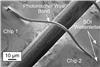 |
| The wire bond is adapted to the position and orientation of the chips. (Figure: N. Lindenmann and G. Balthasar) ((Bildinschriften: Photonic wire bond, SOI waveguide)) |
Abstract:
A team of KIT researchers directed by Professor Christian Koos has succeeded in developing a novel optical connection between semiconductor chips. "Photonic wire bonding" reaches data transmission rates in the range of several terabits per second and is suited perfectly for production on the industrial scale. In the future, this technology may be used in high-performance emitter-receiver systems for optical data transmission and, thus, contribute to reducing energy consumption of the internet. The scientists published their results in the journal "Optics Express".
Optical Waveguide Connects Semiconductor Chips
Karlsruhe, Germany | Posted on September 21st, 2012Communication processes can be made quicker and more energy-efficient with photonic components. Development of high-performance optical emitters and receivers integrated on microchips has already reached a high level. However, there have not yet been any satisfactory possibilities of bridging semiconductor chips optically. "The biggest difficulty consists in aligning the chips precisely such that the waveguides meet," explains Christian Koos, professor at the KIT Institutes of Photonics and Quantum Electronics (IPQ) and of Microstructure Technology (IMT) as well as member of the Center for Functional Nanostructures (CFN).
The team under Christian Koos tackles this problem from the other side: The researchers first fix the chips and then structure a polymer-based optical waveguide in a perfectly fitting manner. To adapt the interconnection to the position and orientation of the chip, the scientists developed a method for the three-dimensional structuring of an optical waveguide. They used so-called two-photon polymerization which reaches a high resolution. A femtosecond laser writes the free-form waveguide structure directly into a polymer that is located on the surface of the chip. For this purpose, the KIT researchers use a laser lithography system made by the Nanoscribe company, a spinoff of KIT.
Prototypes of the photonic wire bonds reached very small losses and a very high transmission bandwidth in the range of infrared telecommunication wavelengths around 1.55 micrometers. In first experiments, the researchers already demonstrated data transmission rates in excess of 5 terabits per second. Potential applications of photonic wire bonds lie in complex emitter-receiver systems for optical telecommunication as well as in sensor and measurement technology. As the highly precise orientation of the chips in manufacturing is no longer required, the process is particularly suited for the automatic production of large series. KIT researchers now plan to transfer this technology to industrial application in cooperation with partner companies.
Full bibliographic informationN. Lindenmann, G. Balthasar, D. Hillerkuss, R. Schmogrow, M. Jordan, J. Leuthold, W. Freude, and C. Koos: Photonic wire bonding: a novel concept for chip-scale interconnects. Optics Express, Vol. 20, No. 16; 30 July 2012.
####
About Karlsruhe Institute of Technology
Karlsruhe Institute of Technology (KIT) is a public corporation according to the legislation of the state of Baden-W�rttemberg. It fulfills the mission of a university and the mission of a national research center of the Helmholtz Association. KIT focuses on a knowledge triangle that links the tasks of research, teaching, and innovation.
For more information, please click here
Contacts:
Monika Landgraf
Karlsruhe Institut of Technology
+49 721 60847414
Copyright © AlphaGalileo
If you have a comment, please Contact us.Issuers of news releases, not 7th Wave, Inc. or Nanotechnology Now, are solely responsible for the accuracy of the content.
Bookmark:


| Related News Press |
News and information
![]() Quantum computer improves AI predictions April 17th, 2026
Quantum computer improves AI predictions April 17th, 2026
![]() Flexible sensor gains sensitivity under pressure April 17th, 2026
Flexible sensor gains sensitivity under pressure April 17th, 2026
![]() A reusable chip for particulate matter sensing April 17th, 2026
A reusable chip for particulate matter sensing April 17th, 2026
![]() Detecting vibrational quantum beating in the predissociation dynamics of SF6 using time-resolved photoelectron spectroscopy April 17th, 2026
Detecting vibrational quantum beating in the predissociation dynamics of SF6 using time-resolved photoelectron spectroscopy April 17th, 2026
Chip Technology
![]() A reusable chip for particulate matter sensing April 17th, 2026
A reusable chip for particulate matter sensing April 17th, 2026
![]() Metasurfaces smooth light to boost magnetic sensing precision January 30th, 2026
Metasurfaces smooth light to boost magnetic sensing precision January 30th, 2026
Optical computing/Photonic computing
![]() ICFO researchers overcome long-standing bottleneck in single photon detection with twisted 2D materials August 8th, 2025
ICFO researchers overcome long-standing bottleneck in single photon detection with twisted 2D materials August 8th, 2025
![]() Programmable electron-induced color router array May 14th, 2025
Programmable electron-induced color router array May 14th, 2025
Discoveries
![]() Quantum computer improves AI predictions April 17th, 2026
Quantum computer improves AI predictions April 17th, 2026
![]() Flexible sensor gains sensitivity under pressure April 17th, 2026
Flexible sensor gains sensitivity under pressure April 17th, 2026
![]() A reusable chip for particulate matter sensing April 17th, 2026
A reusable chip for particulate matter sensing April 17th, 2026
![]() Detecting vibrational quantum beating in the predissociation dynamics of SF6 using time-resolved photoelectron spectroscopy April 17th, 2026
Detecting vibrational quantum beating in the predissociation dynamics of SF6 using time-resolved photoelectron spectroscopy April 17th, 2026
Announcements
![]() A fundamentally new therapeutic approach to cystic fibrosis: Nanobody repairs cellular defect April 17th, 2026
A fundamentally new therapeutic approach to cystic fibrosis: Nanobody repairs cellular defect April 17th, 2026
![]() UC Irvine physicists discover method to reverse �quantum scrambling� : The work addresses the problem of information loss in quantum computing system April 17th, 2026
UC Irvine physicists discover method to reverse �quantum scrambling� : The work addresses the problem of information loss in quantum computing system April 17th, 2026
Photonics/Optics/Lasers
![]() Metasurfaces smooth light to boost magnetic sensing precision January 30th, 2026
Metasurfaces smooth light to boost magnetic sensing precision January 30th, 2026
![]() From sensors to smart systems: the rise of AI-driven photonic noses January 30th, 2026
From sensors to smart systems: the rise of AI-driven photonic noses January 30th, 2026
|
|
||
|
|
||
| The latest news from around the world, FREE | ||
|
|
||
|
|
||
| Premium Products | ||
|
|
||
|
Only the news you want to read!
Learn More |
||
|
|
||
|
Full-service, expert consulting
Learn More |
||
|
|
||