Home > Press > Patterning defect-free nanocrystal films with nanometer resolution: New process developed at MIT could enable better LED displays, solar cells and biosensors — and foster basic physics research
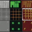 |
| Images of nanopatterned films of nano crystalline material produced by the MIT research team. Each row shows a different pattern produced on films of either cadmium selenide (top and bottom) or a combination of zinc cadmium selenide and zinc cadmium sulfur (middle row). The three images in each row are made using different kinds of microscopes: left to right, scanning electron microscope, optical (showing real-color fluorescence), and atomic force microscope. Images courtesy of Mentzel et al, from Nano Letters |
Abstract:
Films made of semiconductor nanocrystals — tiny crystals measuring just a few billionths of a meter across — are seen as a promising new material for a wide range of applications. Nanocrystals could be used in electronic or photonic circuits, detectors for biomolecules, or the glowing pixels on high-resolution display screens. They also hold promise for more efficient solar cells.
Patterning defect-free nanocrystal films with nanometer resolution: New process developed at MIT could enable better LED displays, solar cells and biosensors — and foster basic physics research
Cambridge, MA | Posted on August 20th, 2012The size of a semiconductor nanocrystal determines its electrical and optical properties. But it's very hard to control the placement of nanocrystals on a surface in order to make structurally uniform films. Typical nanocrystal films also have cracks that limit their usefulness and make it impossible to measure the fundamental properties of these materials.
Now, researchers at MIT say they have found ways of making defect-free patterns of nanocrystal films where the shape and position of the films are controlled with nanoscale resolution, potentially opening up a significant area for research and possible new applications.
"We've been trying to understand how electrons move in arrays of these nanocrystals," which has been difficult with limited control over the formation of the arrays, says physicist Marc Kastner, the Donner Professor of Science, dean of MIT's School of Science and senior author of a paper published online in the journal Nano Letters.
The work builds on research by Moungi Bawendi, the Lester Wolfe Professor of Chemistry at MIT and a co-author of this paper, who was one of the first researchers to precisely control nanocrystal production. Such control made it possible, among other things, to produce materials that glow, or fluoresce, in a range of different colors based on their sizes — even though they are all made of the same material.
In the initial phases of the new work, postdoc Tamar Mentzel produced nanoscale patterns that emit invisible infrared light. But working on such systems is tedious, since each fine-tuning has to be checked using time-consuming electron microscopy. So when Mentzel succeeded in getting semiconductor nanocrystal patterns to glow with visible light, making them visible through an optical microscope, it meant that the team could greatly speed the development of the new technology. "Even though the nanoscale patterns are below the resolution limit of the optical microscope, the nanocrystals act as a light source, rendering them visible," Mentzel says.
The electrical conductivity of the researchers' defect-free films is roughly 180 times greater than that of the cracked films made by conventional methods. In addition, the process developed by the MIT team has already made it possible to create patterns on a silicon surface that are just 30 nanometers across — about the size of the finest features possible with present manufacturing techniques.
The process is unique in producing such tiny patterns of defect-free films, Mentzel says. "The trick was to get the film to be uniform, and to stick" to the silicon dioxide substrate, Kastner adds. That was achieved by leaving a thin layer of polymer to coat the surface before depositing the layer of nanocrystals on top of it. The researchers conjecture that tiny organic molecules on the surface of the nanocrystals help them bind to the polymer layer.
Such nanocrystal patterns could have many applications, Kastner says. Because these nanocrystals can be tuned not only to emit but also to absorb a wide spectrum of colors of light, they could enable a new kind of broad-spectrum solar cell, he says.
But Kastner and Mentzel's personal interest has more to do with basic physics: Since the minuscule crystals behave almost like oversized atoms, the researchers aim to use the arrays to study fundamental processes of solids, Mentzel says. The success of this technique has already enabled new research on how electrons move in the films.
Such materials could also be used to develop sensitive detectors for tiny amounts of certain biological molecules, either as screening systems for toxins or as medical testing devices, the researchers say.
Douglas Natelson, a professor of physics and astronomy at Rice University who was not involved in this work, says, "The challenge in the past has been achieving thin, uniform films, patterned at high resolution, with good contact between the nanocrystals and no cracking." The MIT team's approach, he says, "while deceptively simple in appearance, accomplishes all of these objectives."
Natelson adds: "I think this is a very nice achievement. The fluorescence images showing the nanopatterned films are eye-popping, particularly for those who know how tough this is."
The research was supported by the U.S Army Research Office, the Department of Energy and Samsung.
Written by: David L. Chandler, MIT News Office
####
For more information, please click here
Contacts:
Caroline McCall
MIT News Office
617-253-1682
Copyright © MIT
If you have a comment, please Contact us.Issuers of news releases, not 7th Wave, Inc. or Nanotechnology Now, are solely responsible for the accuracy of the content.
Bookmark:


| Related News Press |
News and information
![]() Quantum computer improves AI predictions April 17th, 2026
Quantum computer improves AI predictions April 17th, 2026
![]() Flexible sensor gains sensitivity under pressure April 17th, 2026
Flexible sensor gains sensitivity under pressure April 17th, 2026
![]() A reusable chip for particulate matter sensing April 17th, 2026
A reusable chip for particulate matter sensing April 17th, 2026
![]() Detecting vibrational quantum beating in the predissociation dynamics of SF6 using time-resolved photoelectron spectroscopy April 17th, 2026
Detecting vibrational quantum beating in the predissociation dynamics of SF6 using time-resolved photoelectron spectroscopy April 17th, 2026
Thin films
![]() Tiny nanosheets, big leap: A new sensor detects ethanol at ultra-low levels January 30th, 2026
Tiny nanosheets, big leap: A new sensor detects ethanol at ultra-low levels January 30th, 2026
Display technology/LEDs/SS Lighting/OLEDs
![]() Spinel-type sulfide semiconductors to operate the next-generation LEDs and solar cells For solar-cell absorbers and green-LED source October 3rd, 2025
Spinel-type sulfide semiconductors to operate the next-generation LEDs and solar cells For solar-cell absorbers and green-LED source October 3rd, 2025
![]() Efficient and stable hybrid perovskite-organic light-emitting diodes with external quantum efficiency exceeding 40 per cent July 5th, 2024
Efficient and stable hybrid perovskite-organic light-emitting diodes with external quantum efficiency exceeding 40 per cent July 5th, 2024
Govt.-Legislation/Regulation/Funding/Policy
![]() Quantum computer improves AI predictions April 17th, 2026
Quantum computer improves AI predictions April 17th, 2026
![]() Metasurfaces smooth light to boost magnetic sensing precision January 30th, 2026
Metasurfaces smooth light to boost magnetic sensing precision January 30th, 2026
![]() New imaging approach transforms study of bacterial biofilms August 8th, 2025
New imaging approach transforms study of bacterial biofilms August 8th, 2025
Chip Technology
![]() A reusable chip for particulate matter sensing April 17th, 2026
A reusable chip for particulate matter sensing April 17th, 2026
![]() Metasurfaces smooth light to boost magnetic sensing precision January 30th, 2026
Metasurfaces smooth light to boost magnetic sensing precision January 30th, 2026
Sensors
![]() Flexible sensor gains sensitivity under pressure April 17th, 2026
Flexible sensor gains sensitivity under pressure April 17th, 2026
![]() Tiny nanosheets, big leap: A new sensor detects ethanol at ultra-low levels January 30th, 2026
Tiny nanosheets, big leap: A new sensor detects ethanol at ultra-low levels January 30th, 2026
![]() From sensors to smart systems: the rise of AI-driven photonic noses January 30th, 2026
From sensors to smart systems: the rise of AI-driven photonic noses January 30th, 2026
![]() Sensors innovations for smart lithium-based batteries: advancements, opportunities, and potential challenges August 8th, 2025
Sensors innovations for smart lithium-based batteries: advancements, opportunities, and potential challenges August 8th, 2025
Discoveries
![]() Quantum computer improves AI predictions April 17th, 2026
Quantum computer improves AI predictions April 17th, 2026
![]() Flexible sensor gains sensitivity under pressure April 17th, 2026
Flexible sensor gains sensitivity under pressure April 17th, 2026
![]() A reusable chip for particulate matter sensing April 17th, 2026
A reusable chip for particulate matter sensing April 17th, 2026
![]() Detecting vibrational quantum beating in the predissociation dynamics of SF6 using time-resolved photoelectron spectroscopy April 17th, 2026
Detecting vibrational quantum beating in the predissociation dynamics of SF6 using time-resolved photoelectron spectroscopy April 17th, 2026
Announcements
![]() A fundamentally new therapeutic approach to cystic fibrosis: Nanobody repairs cellular defect April 17th, 2026
A fundamentally new therapeutic approach to cystic fibrosis: Nanobody repairs cellular defect April 17th, 2026
![]() UC Irvine physicists discover method to reverse ‘quantum scrambling’ : The work addresses the problem of information loss in quantum computing system April 17th, 2026
UC Irvine physicists discover method to reverse ‘quantum scrambling’ : The work addresses the problem of information loss in quantum computing system April 17th, 2026
Military
![]() Quantum engineers ‘squeeze’ laser frequency combs to make more sensitive gas sensors January 17th, 2025
Quantum engineers ‘squeeze’ laser frequency combs to make more sensitive gas sensors January 17th, 2025
![]() Chainmail-like material could be the future of armor: First 2D mechanically interlocked polymer exhibits exceptional flexibility and strength January 17th, 2025
Chainmail-like material could be the future of armor: First 2D mechanically interlocked polymer exhibits exceptional flexibility and strength January 17th, 2025
![]() Single atoms show their true color July 5th, 2024
Single atoms show their true color July 5th, 2024
![]() NRL charters Navy’s quantum inertial navigation path to reduce drift April 5th, 2024
NRL charters Navy’s quantum inertial navigation path to reduce drift April 5th, 2024
Energy
![]() Sensors innovations for smart lithium-based batteries: advancements, opportunities, and potential challenges August 8th, 2025
Sensors innovations for smart lithium-based batteries: advancements, opportunities, and potential challenges August 8th, 2025
![]() Simple algorithm paired with standard imaging tool could predict failure in lithium metal batteries August 8th, 2025
Simple algorithm paired with standard imaging tool could predict failure in lithium metal batteries August 8th, 2025
Photonics/Optics/Lasers
![]() Metasurfaces smooth light to boost magnetic sensing precision January 30th, 2026
Metasurfaces smooth light to boost magnetic sensing precision January 30th, 2026
![]() From sensors to smart systems: the rise of AI-driven photonic noses January 30th, 2026
From sensors to smart systems: the rise of AI-driven photonic noses January 30th, 2026
Solar/Photovoltaic
![]() Spinel-type sulfide semiconductors to operate the next-generation LEDs and solar cells For solar-cell absorbers and green-LED source October 3rd, 2025
Spinel-type sulfide semiconductors to operate the next-generation LEDs and solar cells For solar-cell absorbers and green-LED source October 3rd, 2025
![]() KAIST researchers introduce new and improved, next-generation perovskite solar cell November 8th, 2024
KAIST researchers introduce new and improved, next-generation perovskite solar cell November 8th, 2024
![]() Groundbreaking precision in single-molecule optoelectronics August 16th, 2024
Groundbreaking precision in single-molecule optoelectronics August 16th, 2024
![]() Development of zinc oxide nanopagoda array photoelectrode: photoelectrochemical water-splitting hydrogen production January 12th, 2024
Development of zinc oxide nanopagoda array photoelectrode: photoelectrochemical water-splitting hydrogen production January 12th, 2024
|
|
||
|
|
||
| The latest news from around the world, FREE | ||
|
|
||
|
|
||
| Premium Products | ||
|
|
||
|
Only the news you want to read!
Learn More |
||
|
|
||
|
Full-service, expert consulting
Learn More |
||
|
|
||