Home > Press > New Affordable Scanning Probe Microscope with Advanced Capabilities
 |
Abstract:
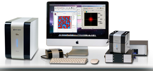
NT-MDT announced the release of the SOLVER Nano Scanning Probe Microscope (SPM). The SOLVER Nano is an affordable SPM with advanced measurement capabilities. The SOLVER Nano offers research capability at a low cost of ownership.
New Affordable Scanning Probe Microscope with Advanced Capabilities
Moscow, Russia | Posted on January 31st, 2012NT-MDT announces that it has released the SOLVER Nano SPM. The Solver Nano is an SPM that offers advanced features and capability for users with research needs or for new SPM users in an ergonomic compact design at an affordable price.
The SOLVER Nano is a complete SPM, offering Atomic Force Microscopy (AFM) and Scanning Tunneling Microscopy (STM) techniques. Notable features include advanced software, digital control electronics, easy to align AFM probe holder design and optional educational measuring head for teaching purposes.
The system comes with many advanced imaging modes built in including Scanning Kelvin Probe Microscopy (SKM), Magnetic Force Microscopy (MFM), Scanning Spreading Resistance Imaging (SSRM), Piezo Force Microscopy (PFM) and 100 micron x 100 micron closed-loop high resolution scanner. Due to ScanScaler TM option the same scanner can be easily adjusted for atomic level resolution.
The SOLVER Nano complements NT-MDT's complete line of AFM products, by offering advanced research capability in an affordable, compact and easy to use SPM system.
####
About NT-MDT
Our mission is to enable researchers, engineers and developers to conduct nanoscale research by creating ever more perfect nanotechnology instrumentation. Along the way, we maintain a global perspective, always taking into consideration the needs of student in the classroom, the researcher at the cutting edge in the laboratory, and the practicalities of industrial R&D.
For more information, please click here
Contacts:
NT-MDT Co. Building 100
Zelenograd, Moscow 124482, Russia
Phone: +7 (499) 735-7777
Fax: +7 (499) 735-6410
Copyright © NT-MDT
If you have a comment, please Contact us.Issuers of news releases, not 7th Wave, Inc. or Nanotechnology Now, are solely responsible for the accuracy of the content.
| Related News Press |
News and information
![]() Quantum computer improves AI predictions April 17th, 2026
Quantum computer improves AI predictions April 17th, 2026
![]() Flexible sensor gains sensitivity under pressure April 17th, 2026
Flexible sensor gains sensitivity under pressure April 17th, 2026
![]() A reusable chip for particulate matter sensing April 17th, 2026
A reusable chip for particulate matter sensing April 17th, 2026
![]() Detecting vibrational quantum beating in the predissociation dynamics of SF6 using time-resolved photoelectron spectroscopy April 17th, 2026
Detecting vibrational quantum beating in the predissociation dynamics of SF6 using time-resolved photoelectron spectroscopy April 17th, 2026
Imaging
![]() Simple algorithm paired with standard imaging tool could predict failure in lithium metal batteries August 8th, 2025
Simple algorithm paired with standard imaging tool could predict failure in lithium metal batteries August 8th, 2025
Announcements
![]() A fundamentally new therapeutic approach to cystic fibrosis: Nanobody repairs cellular defect April 17th, 2026
A fundamentally new therapeutic approach to cystic fibrosis: Nanobody repairs cellular defect April 17th, 2026
![]() UC Irvine physicists discover method to reverse �quantum scrambling� : The work addresses the problem of information loss in quantum computing system April 17th, 2026
UC Irvine physicists discover method to reverse �quantum scrambling� : The work addresses the problem of information loss in quantum computing system April 17th, 2026
Tools
![]() Metasurfaces smooth light to boost magnetic sensing precision January 30th, 2026
Metasurfaces smooth light to boost magnetic sensing precision January 30th, 2026
![]() From sensors to smart systems: the rise of AI-driven photonic noses January 30th, 2026
From sensors to smart systems: the rise of AI-driven photonic noses January 30th, 2026
![]() Japan launches fully domestically produced quantum computer: Expo visitors to experience quantum computing firsthand August 8th, 2025
Japan launches fully domestically produced quantum computer: Expo visitors to experience quantum computing firsthand August 8th, 2025
|
|
||
|
|
||
| The latest news from around the world, FREE | ||
|
|
||
|
|
||
| Premium Products | ||
|
|
||
|
Only the news you want to read!
Learn More |
||
|
|
||
|
Full-service, expert consulting
Learn More |
||
|
|
||


