Home > Press > UCSB Researchers Uncover Transparency Limits on Transparent Conducting Oxides: Computational Materials researchers at UC Santa Barbara use cutting-edge calculations to determine fundamental optical transparency limits in conducting oxide material tin oxide
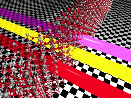 |
| Three beams of light (red for infrared, yellow for visible light, and violet for ultraviolet) travel through a layer of SnO2. Absorption by the conduction electrons in the oxide reduces the intensity of the beams. Credit: Hartwin Peelaers, UCSB |
Abstract:
Researchers in the Computational Materials Group at the University of California, Santa Barbara (UCSB) have uncovered the fundamental limits on optical transparency in the class of materials known as transparent conducting oxides. Their discovery will support development of energy efficiency improvements for devices that depend on optoelectronic technology, such as light- emitting diodes and solar cells.
UCSB Researchers Uncover Transparency Limits on Transparent Conducting Oxides: Computational Materials researchers at UC Santa Barbara use cutting-edge calculations to determine fundamental optical transparency limits in conducting oxide material tin oxide
Santa Barbara, CA | Posted on January 18th, 2012Transparent conducting oxides are used as transparent contacts in a wide range of optoelectronic devices, such as photovoltaic cells, light-emitting diodes (LEDs), and LCD touch screens. These materials are unique in that they can conduct electricity while being transparent to visible light. For optoelectronic devices to be able to emit or absorb light, it is important that the electrical contacts at the top of the device are optically transparent. Opaque metals and most transparent materials lack the balance between these two characteristics to be functional for use in such technology.
In a paper published in Applied Physics Letters [APL 100, 011914 (2012)], the UCSB researchers used cutting-edge calculation methods to investigate tin dioxide (SnO2), a widely-used conducting oxide.
Conducting oxides strike an ideal balance between transparency and conductivity because their wide band gaps prevent absorption of visible light by excitation of electrons across the gap, according to the researchers. At the same time, dopant atoms provide additional electrons in the conduction band that enable electrical conductivity. However, these free electrons can also absorb light by being excited to higher conduction-band states.
"Direct absorption of visible light cannot occur in these materials because the next available electron level is too high in energy. But we found that more complex absorption mechanisms, which also involve lattice vibrations, can be remarkably strong", says Hartwin Peelaers, a postdoctoral researcher and the lead author of the paper. The other authors are Emmanouil Kioupakis, now at the University of Michigan, and Chris Van de Walle, a professor in the UCSB Materials Department and head of the research group.
They found that tin dioxide only weakly absorbs visible light, thus letting most light pass through, so that it is still a useful transparent contact. In their study, the transparency of SnO2 declined when moving to other wavelength regions. Absorption was 5 times stronger for ultraviolet light and 20 times stronger for the infrared light used in telecommunications.
"Every bit of light that gets absorbed reduces the efficiency of a solar cell or LED", remarked Chris Van de Walle. "Understanding what causes the absorption is essential for engineering improved materials to be used in more efficient devices."
Van de Walle's Computational Materials Group is affiliated with the College of Engineering at UCSB. Their research explores semiconducting binary oxides, nitride semiconductors, novel channel materials and dielectrics, materials for quantum computing, photochemical hydrogen generation, and metallic nanoparticles. Learn more about Computational Materials research at www.mrl.ucsb.edu/~vandewalle .
Their research was supported as part of the UCSB Center for Energy Efficient Materials, an Energy Frontier Research Center funded by the United States Department of Energy, by the Belgian American Educational Foundation, and by the UCSB Materials Research Laboratory: a National Science Foundation MRSEC.
####
For more information, please click here
Contacts:
Melissa Van De Werfhorst
Communications Manager
UCSB College of Engineering
(805) 893-4301
Copyright © University of California, Santa Barbara (UCSB)
If you have a comment, please Contact us.Issuers of news releases, not 7th Wave, Inc. or Nanotechnology Now, are solely responsible for the accuracy of the content.
Bookmark:


| Related Links |
![]() Faculty Profile - Chris Van de Walle:
Faculty Profile - Chris Van de Walle:
![]() UCSB Computation Materials Group:
UCSB Computation Materials Group:
![]() Applied Physics Letters Paper:
Applied Physics Letters Paper:
![]() Download this release as a .pdf:
Download this release as a .pdf:
| Related News Press |
News and information
![]() Quantum computer improves AI predictions April 17th, 2026
Quantum computer improves AI predictions April 17th, 2026
![]() Flexible sensor gains sensitivity under pressure April 17th, 2026
Flexible sensor gains sensitivity under pressure April 17th, 2026
![]() A reusable chip for particulate matter sensing April 17th, 2026
A reusable chip for particulate matter sensing April 17th, 2026
![]() Detecting vibrational quantum beating in the predissociation dynamics of SF6 using time-resolved photoelectron spectroscopy April 17th, 2026
Detecting vibrational quantum beating in the predissociation dynamics of SF6 using time-resolved photoelectron spectroscopy April 17th, 2026
Display technology/LEDs/SS Lighting/OLEDs
![]() Spinel-type sulfide semiconductors to operate the next-generation LEDs and solar cells For solar-cell absorbers and green-LED source October 3rd, 2025
Spinel-type sulfide semiconductors to operate the next-generation LEDs and solar cells For solar-cell absorbers and green-LED source October 3rd, 2025
![]() Efficient and stable hybrid perovskite-organic light-emitting diodes with external quantum efficiency exceeding 40 per cent July 5th, 2024
Efficient and stable hybrid perovskite-organic light-emitting diodes with external quantum efficiency exceeding 40 per cent July 5th, 2024
Govt.-Legislation/Regulation/Funding/Policy
![]() Quantum computer improves AI predictions April 17th, 2026
Quantum computer improves AI predictions April 17th, 2026
![]() Metasurfaces smooth light to boost magnetic sensing precision January 30th, 2026
Metasurfaces smooth light to boost magnetic sensing precision January 30th, 2026
![]() New imaging approach transforms study of bacterial biofilms August 8th, 2025
New imaging approach transforms study of bacterial biofilms August 8th, 2025
Chip Technology
![]() A reusable chip for particulate matter sensing April 17th, 2026
A reusable chip for particulate matter sensing April 17th, 2026
![]() Metasurfaces smooth light to boost magnetic sensing precision January 30th, 2026
Metasurfaces smooth light to boost magnetic sensing precision January 30th, 2026
Announcements
![]() A fundamentally new therapeutic approach to cystic fibrosis: Nanobody repairs cellular defect April 17th, 2026
A fundamentally new therapeutic approach to cystic fibrosis: Nanobody repairs cellular defect April 17th, 2026
![]() UC Irvine physicists discover method to reverse �quantum scrambling� : The work addresses the problem of information loss in quantum computing system April 17th, 2026
UC Irvine physicists discover method to reverse �quantum scrambling� : The work addresses the problem of information loss in quantum computing system April 17th, 2026
Energy
![]() Sensors innovations for smart lithium-based batteries: advancements, opportunities, and potential challenges August 8th, 2025
Sensors innovations for smart lithium-based batteries: advancements, opportunities, and potential challenges August 8th, 2025
![]() Simple algorithm paired with standard imaging tool could predict failure in lithium metal batteries August 8th, 2025
Simple algorithm paired with standard imaging tool could predict failure in lithium metal batteries August 8th, 2025
Solar/Photovoltaic
![]() Spinel-type sulfide semiconductors to operate the next-generation LEDs and solar cells For solar-cell absorbers and green-LED source October 3rd, 2025
Spinel-type sulfide semiconductors to operate the next-generation LEDs and solar cells For solar-cell absorbers and green-LED source October 3rd, 2025
![]() KAIST researchers introduce new and improved, next-generation perovskite solar cell November 8th, 2024
KAIST researchers introduce new and improved, next-generation perovskite solar cell November 8th, 2024
![]() Groundbreaking precision in single-molecule optoelectronics August 16th, 2024
Groundbreaking precision in single-molecule optoelectronics August 16th, 2024
![]() Development of zinc oxide nanopagoda array photoelectrode: photoelectrochemical water-splitting hydrogen production January 12th, 2024
Development of zinc oxide nanopagoda array photoelectrode: photoelectrochemical water-splitting hydrogen production January 12th, 2024
|
|
||
|
|
||
| The latest news from around the world, FREE | ||
|
|
||
|
|
||
| Premium Products | ||
|
|
||
|
Only the news you want to read!
Learn More |
||
|
|
||
|
Full-service, expert consulting
Learn More |
||
|
|
||