Home > Press > Sorting out the nanotubes, for better electronics
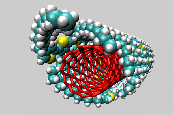 |
| Francois Gygi and Giulia Galli / UC-Davis A computer-generated cross section of the polymer-coated carbon nanotube. The polymer shell (blue) wraps around a semiconducting single-walled carbon nanotube (red). |
Abstract:
A new technique developed by Stanford researchers advances commercial potential of semiconducting carbon nanotubes for printable circuits, bendable display screens, stretchable electronics and solar technology.
Sorting out the nanotubes, for better electronics
Stanford, CA | Posted on November 18th, 2011BY SARAH JANE KELLER
Carbon nanotubes could make many electronic devices cheaper and more efficient. But when nanotubes are manufactured, tubes that work for solar cells are mixed with tubes that work for batteries. The final product is a nanotube powder that is not ideal for any single commercial application.
Zhenan Bao, Stanford associate professor of chemical engineering, and her colleagues at University of California-Davis and the Samsung Advanced Institute of Technology have discovered a technique to selectively sort semiconducting single-walled carbon nanotubes from the mixture. The results appear online in Nature Communications.
The semiconducting nanotubes could be used in flexible transistors for other technologies that Bao's group develops, including circuits printed on plastic, bendable display screens and stretchable electronics. The nanotubes could also close gaps in solar cell technology.
"Sorting has been a major bottleneck for carbon nanotubes to be viable for practical electronics applications," Bao said. "This work solves the problem of separating the conducting from the semiconducting nanotubes."
Conducting tubes are used in wires and electrodes but semiconducting tubes are the active material for transistors or solar cells. Mixtures of conducting and semiconducting tubes do not carry enough current for wires or battery electrodes. And when the mixture is used for semiconducting, as in a transistor, the excess current from the conducting nanotubes will short the device.
Bao's group uses a polymer that selectively sorts the mixture by wrapping around semiconducting nanotubes, and not conducting nanotubes. Mixing the polymer with commercially available carbon nanotubes in a solvent separates semiconducting tubes from conducting tubes.
In her past work with the polymer, Bao was the first to find that it has good semiconducting properties in transistors. It is now the most widely studied polymer for plastic circuits and plastic transistors and also for plastic solar cells. Bao's group is the first to combine it with semiconducting carbon nanotubes.
This is not the first time a polymer has been used to sort conducting and semiconducting nanotubes. However, past polymers have insulated the nanotubes and required extensive removal treatments to restore the conductivity of the nanotubes.
The polymer in Bao's process does not need to be removed. The final product is a semiconducting nanotube and polymer ink that can be used to make printable electronics.
"Our simple process allows us to build useful devices very easily," she said.
The group tested nearly 200 individual nanotubes to confirm that the polymer only wraps around semiconducting tubes and not conducting tubes. To explain how the polymer wraps around the carbon nanotube, UC-Davis collaborators Giulia Galli and Francois Gygi modeled the geometry of a semiconducting carbon nanotube and its polymer shell.
According to Galli, the model provides "a theoretical explanation of how this polymer actually interacts with the nanotube." The polymer has a long, rigid backbone, with regular arm-like molecular chains along each side. The side chains fit together like fingers, making a ribbon of polymer that wraps around the semiconducting nanotubes.
Bao's work with nanotubes is part of her long-term collaboration with the Samsung Advanced Institute of Technology. "I'm especially happy that this polymer can now be used to sort nanotubes," Bao said. "It merges two very important materials together and makes a hybrid material that could be very useful for printed and flexible electronics."
Jeffrey B.-H. Tok, senior research engineer; Andrew Spakowitz, assistant professor of chemical engineering; and H.S.Philip Wong, professor of electrical engineering, contributed to the research. Chemical engineering graduate student Hang Woo Lee, materials science and engineering graduate students Steve Park and Huiliang Wang also contributed, as well as Satoshi Morishita of chemical engineering,
Luckshitha S. Liyanage of electrical engineering and Nishant Patil of electrical engineering.
The Samsung Advanced Institute of Technology and the National Science Foundation provided funding for the research.
Sarah Jane Keller is a science-writing intern at the Stanford News Service.
####
For more information, please click here
Contacts:
Zhenan Bao
Department of Chemical Engineering
(650) 723-2419
Dan Stober
Stanford News Service:
(650) 721-6965
Copyright © Stanford University
If you have a comment, please Contact us.Issuers of news releases, not 7th Wave, Inc. or Nanotechnology Now, are solely responsible for the accuracy of the content.
Bookmark:


| Related News Press |
News and information
![]() Quantum computer improves AI predictions April 17th, 2026
Quantum computer improves AI predictions April 17th, 2026
![]() Flexible sensor gains sensitivity under pressure April 17th, 2026
Flexible sensor gains sensitivity under pressure April 17th, 2026
![]() A reusable chip for particulate matter sensing April 17th, 2026
A reusable chip for particulate matter sensing April 17th, 2026
![]() Detecting vibrational quantum beating in the predissociation dynamics of SF6 using time-resolved photoelectron spectroscopy April 17th, 2026
Detecting vibrational quantum beating in the predissociation dynamics of SF6 using time-resolved photoelectron spectroscopy April 17th, 2026
Flexible Electronics
![]() Flexible sensor gains sensitivity under pressure April 17th, 2026
Flexible sensor gains sensitivity under pressure April 17th, 2026
![]() Flexible electronics integrated with paper-thin structure for use in space January 17th, 2025
Flexible electronics integrated with paper-thin structure for use in space January 17th, 2025
Display technology/LEDs/SS Lighting/OLEDs
![]() Spinel-type sulfide semiconductors to operate the next-generation LEDs and solar cells For solar-cell absorbers and green-LED source October 3rd, 2025
Spinel-type sulfide semiconductors to operate the next-generation LEDs and solar cells For solar-cell absorbers and green-LED source October 3rd, 2025
Chip Technology
![]() A reusable chip for particulate matter sensing April 17th, 2026
A reusable chip for particulate matter sensing April 17th, 2026
![]() Metasurfaces smooth light to boost magnetic sensing precision January 30th, 2026
Metasurfaces smooth light to boost magnetic sensing precision January 30th, 2026
Nanotubes/Buckyballs/Fullerenes/Nanorods/Nanostrings/Nanosheets
![]() Tiny nanosheets, big leap: A new sensor detects ethanol at ultra-low levels January 30th, 2026
Tiny nanosheets, big leap: A new sensor detects ethanol at ultra-low levels January 30th, 2026
![]() Enhancing power factor of p- and n-type single-walled carbon nanotubes April 25th, 2025
Enhancing power factor of p- and n-type single-walled carbon nanotubes April 25th, 2025
![]() Chainmail-like material could be the future of armor: First 2D mechanically interlocked polymer exhibits exceptional flexibility and strength January 17th, 2025
Chainmail-like material could be the future of armor: First 2D mechanically interlocked polymer exhibits exceptional flexibility and strength January 17th, 2025
![]() Innovative biomimetic superhydrophobic coating combines repair and buffering properties for superior anti-erosion December 13th, 2024
Innovative biomimetic superhydrophobic coating combines repair and buffering properties for superior anti-erosion December 13th, 2024
Nanoelectronics
![]() Lab to industry: InSe wafer-scale breakthrough for future electronics August 8th, 2025
Lab to industry: InSe wafer-scale breakthrough for future electronics August 8th, 2025
![]() Interdisciplinary: Rice team tackles the future of semiconductors Multiferroics could be the key to ultralow-energy computing October 6th, 2023
Interdisciplinary: Rice team tackles the future of semiconductors Multiferroics could be the key to ultralow-energy computing October 6th, 2023
![]() Key element for a scalable quantum computer: Physicists from Forschungszentrum J�lich and RWTH Aachen University demonstrate electron transport on a quantum chip September 23rd, 2022
Key element for a scalable quantum computer: Physicists from Forschungszentrum J�lich and RWTH Aachen University demonstrate electron transport on a quantum chip September 23rd, 2022
![]() Reduced power consumption in semiconductor devices September 23rd, 2022
Reduced power consumption in semiconductor devices September 23rd, 2022
Discoveries
![]() Quantum computer improves AI predictions April 17th, 2026
Quantum computer improves AI predictions April 17th, 2026
![]() Flexible sensor gains sensitivity under pressure April 17th, 2026
Flexible sensor gains sensitivity under pressure April 17th, 2026
![]() A reusable chip for particulate matter sensing April 17th, 2026
A reusable chip for particulate matter sensing April 17th, 2026
![]() Detecting vibrational quantum beating in the predissociation dynamics of SF6 using time-resolved photoelectron spectroscopy April 17th, 2026
Detecting vibrational quantum beating in the predissociation dynamics of SF6 using time-resolved photoelectron spectroscopy April 17th, 2026
Announcements
![]() A fundamentally new therapeutic approach to cystic fibrosis: Nanobody repairs cellular defect April 17th, 2026
A fundamentally new therapeutic approach to cystic fibrosis: Nanobody repairs cellular defect April 17th, 2026
![]() UC Irvine physicists discover method to reverse �quantum scrambling� : The work addresses the problem of information loss in quantum computing system April 17th, 2026
UC Irvine physicists discover method to reverse �quantum scrambling� : The work addresses the problem of information loss in quantum computing system April 17th, 2026
Energy
![]() Sensors innovations for smart lithium-based batteries: advancements, opportunities, and potential challenges August 8th, 2025
Sensors innovations for smart lithium-based batteries: advancements, opportunities, and potential challenges August 8th, 2025
![]() Simple algorithm paired with standard imaging tool could predict failure in lithium metal batteries August 8th, 2025
Simple algorithm paired with standard imaging tool could predict failure in lithium metal batteries August 8th, 2025
Solar/Photovoltaic
![]() Spinel-type sulfide semiconductors to operate the next-generation LEDs and solar cells For solar-cell absorbers and green-LED source October 3rd, 2025
Spinel-type sulfide semiconductors to operate the next-generation LEDs and solar cells For solar-cell absorbers and green-LED source October 3rd, 2025
![]() KAIST researchers introduce new and improved, next-generation perovskite solar cell November 8th, 2024
KAIST researchers introduce new and improved, next-generation perovskite solar cell November 8th, 2024
![]() Groundbreaking precision in single-molecule optoelectronics August 16th, 2024
Groundbreaking precision in single-molecule optoelectronics August 16th, 2024
![]() Development of zinc oxide nanopagoda array photoelectrode: photoelectrochemical water-splitting hydrogen production January 12th, 2024
Development of zinc oxide nanopagoda array photoelectrode: photoelectrochemical water-splitting hydrogen production January 12th, 2024
Printing/Lithography/Inkjet/Inks/Bio-printing/Dyes
![]() Presenting: Ultrasound-based printing of 3D materials�potentially inside the body December 8th, 2023
Presenting: Ultrasound-based printing of 3D materials�potentially inside the body December 8th, 2023
![]() Simple ballpoint pen can write custom LEDs August 11th, 2023
Simple ballpoint pen can write custom LEDs August 11th, 2023
![]() Disposable electronics on a simple sheet of paper October 7th, 2022
Disposable electronics on a simple sheet of paper October 7th, 2022
|
|
||
|
|
||
| The latest news from around the world, FREE | ||
|
|
||
|
|
||
| Premium Products | ||
|
|
||
|
Only the news you want to read!
Learn More |
||
|
|
||
|
Full-service, expert consulting
Learn More |
||
|
|
||