Home > Press > Graphene and friends: A new method to make 2D materials
 |
| http://dx.doi.org/10.1002/anie.201106004|Z. Zeng, Angew. Chem. Int. Ed. ; DOI: 10.1002/anie.201106004 |
Abstract:
by Adrian Miller
Although graphene has had materials researcher hearts racing more or less since its discovery, many scientists see it as just the beginning - if other materials could be processed in the same way, they ask, couldn't it mean a revolution in nanodevice design? Imagine a range of two-dimensional materials, each with their own unique thermal, electronic, optical, and mechanical properties, used for a whole host of nanotechnology applications.
Graphene and friends: A new method to make 2D materials
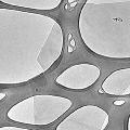
Germany | Posted on November 10th, 2011The problem with this vision - at least, up until now - is that graphene is the only 2D material that can be reliably and easily synthesized in large enough quantities to be useful for device manufacture. Other compounds, for example MoS2 and WS2, are right up there with graphite in terms of potential, but the groups working on their processing haven't been able to move past small scale methods such as mechanical cleavage (� la Geim and Novoselov) and nanotube "unzipping".
However, that might be about to change - last week, a Singaporean team reported a new process to create large numbers of single-layer nanosheets quickly and efficiently, applicable to any suitable bulk material. By inducing lithiation with an electrochemical setup, the materials can be carefully monitored and put into a state ideal for ultrasonication and exfoliation. In less than six hours, and at room temperatures, their test setup obtained an MoS2 nanosheet yield of 92%.
To demonstrate how useful these sheets could be, the team went on to create a proof-of-concept nitric oxide detector from these single MoS2 layers. As they're electrically conductive over large areas, and act as p-type semiconductors, they respond electronically to different NO concentrations, and the addition of gold electrodes meant that the response could measured. This experimental device showed great promise - a detection limit of 190 ppt, definitely well within the limits for a promising sensing platform.
Other, similar, experiments yielded similar results with WS2, TiS2, and others - even graphene! - and the researchers see their method as one that could be adopted to produce a range of 2D nanosheets, for application in areas such as electronics, catalysis, and sensing.
####
For more information, please click here
Copyright © Wiley-VCH Materials Science Journals
If you have a comment, please Contact us.Issuers of news releases, not 7th Wave, Inc. or Nanotechnology Now, are solely responsible for the accuracy of the content.
Bookmark:


| Related News Press |
News and information
![]() Quantum computer improves AI predictions April 17th, 2026
Quantum computer improves AI predictions April 17th, 2026
![]() Flexible sensor gains sensitivity under pressure April 17th, 2026
Flexible sensor gains sensitivity under pressure April 17th, 2026
![]() A reusable chip for particulate matter sensing April 17th, 2026
A reusable chip for particulate matter sensing April 17th, 2026
![]() Detecting vibrational quantum beating in the predissociation dynamics of SF6 using time-resolved photoelectron spectroscopy April 17th, 2026
Detecting vibrational quantum beating in the predissociation dynamics of SF6 using time-resolved photoelectron spectroscopy April 17th, 2026
Chemistry
![]() Projecting light to dispense liquids: A new route to ultra-precise microdroplets January 30th, 2026
Projecting light to dispense liquids: A new route to ultra-precise microdroplets January 30th, 2026
![]() From sensors to smart systems: the rise of AI-driven photonic noses January 30th, 2026
From sensors to smart systems: the rise of AI-driven photonic noses January 30th, 2026
![]() "Nanoreactor" cage uses visible light for catalytic and ultra-selective cross-cycloadditions October 3rd, 2025
"Nanoreactor" cage uses visible light for catalytic and ultra-selective cross-cycloadditions October 3rd, 2025
![]() Cambridge chemists discover simple way to build bigger molecules � one carbon at a time June 6th, 2025
Cambridge chemists discover simple way to build bigger molecules � one carbon at a time June 6th, 2025
![]() Single-atom catalysts change spin state when boosted by a magnetic field June 4th, 2025
Single-atom catalysts change spin state when boosted by a magnetic field June 4th, 2025
Graphene/ Graphite
![]() Electrifying results shed light on graphene foam as a potential material for lab grown cartilage June 6th, 2025
Electrifying results shed light on graphene foam as a potential material for lab grown cartilage June 6th, 2025
![]() Breakthrough in proton barrier films using pore-free graphene oxide: Kumamoto University researchers achieve new milestone in advanced coating technologies September 13th, 2024
Breakthrough in proton barrier films using pore-free graphene oxide: Kumamoto University researchers achieve new milestone in advanced coating technologies September 13th, 2024
Chip Technology
![]() A reusable chip for particulate matter sensing April 17th, 2026
A reusable chip for particulate matter sensing April 17th, 2026
![]() Metasurfaces smooth light to boost magnetic sensing precision January 30th, 2026
Metasurfaces smooth light to boost magnetic sensing precision January 30th, 2026
Sensors
![]() Flexible sensor gains sensitivity under pressure April 17th, 2026
Flexible sensor gains sensitivity under pressure April 17th, 2026
![]() Tiny nanosheets, big leap: A new sensor detects ethanol at ultra-low levels January 30th, 2026
Tiny nanosheets, big leap: A new sensor detects ethanol at ultra-low levels January 30th, 2026
![]() From sensors to smart systems: the rise of AI-driven photonic noses January 30th, 2026
From sensors to smart systems: the rise of AI-driven photonic noses January 30th, 2026
![]() Sensors innovations for smart lithium-based batteries: advancements, opportunities, and potential challenges August 8th, 2025
Sensors innovations for smart lithium-based batteries: advancements, opportunities, and potential challenges August 8th, 2025
Discoveries
![]() Quantum computer improves AI predictions April 17th, 2026
Quantum computer improves AI predictions April 17th, 2026
![]() Flexible sensor gains sensitivity under pressure April 17th, 2026
Flexible sensor gains sensitivity under pressure April 17th, 2026
![]() A reusable chip for particulate matter sensing April 17th, 2026
A reusable chip for particulate matter sensing April 17th, 2026
![]() Detecting vibrational quantum beating in the predissociation dynamics of SF6 using time-resolved photoelectron spectroscopy April 17th, 2026
Detecting vibrational quantum beating in the predissociation dynamics of SF6 using time-resolved photoelectron spectroscopy April 17th, 2026
Announcements
![]() A fundamentally new therapeutic approach to cystic fibrosis: Nanobody repairs cellular defect April 17th, 2026
A fundamentally new therapeutic approach to cystic fibrosis: Nanobody repairs cellular defect April 17th, 2026
![]() UC Irvine physicists discover method to reverse �quantum scrambling� : The work addresses the problem of information loss in quantum computing system April 17th, 2026
UC Irvine physicists discover method to reverse �quantum scrambling� : The work addresses the problem of information loss in quantum computing system April 17th, 2026
|
|
||
|
|
||
| The latest news from around the world, FREE | ||
|
|
||
|
|
||
| Premium Products | ||
|
|
||
|
Only the news you want to read!
Learn More |
||
|
|
||
|
Full-service, expert consulting
Learn More |
||
|
|
||